[popupwfancybox id=”8″]
Time to Take the Next Step
Memristor crossbars, and memristors in general, can be difficult to work with. Outside of well equipped university and government labs its difficult to get hands-on experience. The equipment needed to fabricate and test the devices can be hard to come by and, more often than not, ridiculously expensive. For some years now Knowm has offered the Memristor Discovery introductory academic kits, an inexpensive PCB board, memristor chip and user manual intended to be paired with the Diligent Analog Discovery 2 (AD2). While Memristor Discovery is perfect for gathering experience with a small number of memristors, I felt it was time to take the next step. Over the last few months I set my attention on the design and fabrication of a new memristor research and education platform that pairs with a Raspberry Pi single board computer. The platform enables anyone with an internet connection to gain access to thousands of memristors across 12 to 192 crossbars, depending on how it’s configured. I call it a “kT-RAM Server”.
In this post I will review some key concepts of kT-RAM and the “Unit Crossbar” concept, followed by a review of the build and preliminary testing of the new kT-RAM Raspberry Pi Server.
The platform enables anyone with an internet connection to gain access to thousands of memristors across 12 to 192 crossbars, depending on how it’s configured.
kT-RAM Raspberry Pi Memristor Server
Why Memristors are Exciting
Memristors offer one of the clearest paths to what I call “effective intelligence”, the end game in the artificial intelligence race. For AI to be effective it must (1) actually work from an algorithmic perspective or what I call “primary performance” and (2) it must be space, volume and power efficient, what I call “secondary performance”. While modern machine learning is mostly about separating training/learning from inference, intelligence is synonymous with learning. That is, the end-game in the AI arms race is about building the most effective learning processors. Continuous online learning, at scale, in a small and power efficient package–otherwise known as a “brain”. Of course, the enormous scale of modern record-setting neural network algorithms, and the enormous scale of biological brains, points to an undeniable fact: effective AI processors will need to be very power efficient. A back-of-the-envelop calculation is all one needs to see were we are headed.
Energy is largely expended in computation not by logic itself, but by the movement of information between logic steps and especially to and from memory. We can estimate the energy expended in charging wires when we access synaptic memory. We just assume that we have some number of synapses, each with some bit precision, which we must access over wires that must be charged and discharged as information flows.
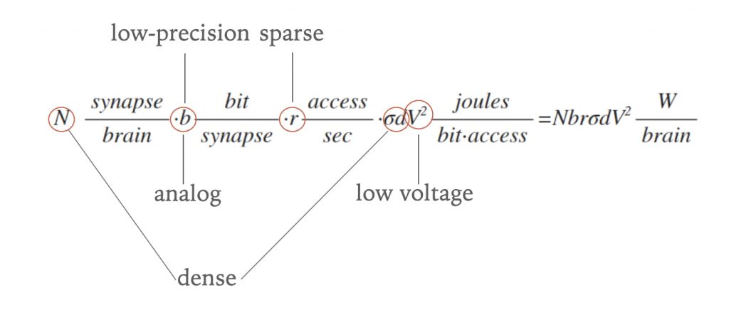
Equation for power of a synaptic processor.
The equation tells a simple story. Synaptic processors are going to be dense, where the separation between synaptic memory and logic will be very small or zero. Synaptic weights will be low-precision or analog. Activity patterns will be sparse, in that not all inputs to a neuron will be active at the same time. The operating voltage will be very low, both for learning and inference. In regards to learning, this introduced an interesting problem I call the “adaptive power problem”. Outside of a breakthrough technology that operates outside the bounds of normal electronics, end-game electronic synaptic processors will have these traits. I do not believe that breakthrough will be quantum computing (not practical) nor optical computing (photons don’t like to interact, required for learning), at least when it comes to learning synaptic processors.

General agreement on the direction of AI hardware.
It’s not a mystery where we are all going, and we all more-or-less agree. Once the algorithm works (“primary performance”), people will compete to make it efficient and inexpensive (“secondary performance”). All of these buzzwords like “sparsity”, “reduced precision”, “analog”, “novel memory”, etc, have their roots in the above equation. When Google guy talks of a “sparsity framework that enables novel memory and compute structures” or Intel guy talks about “better use of memory and sparsity, precision and analog”, they are each just taking stock of the the problem and realizing that the answer obviously lies in a certain direction, specifically the one defined by that simple equation above. I call our work in realizing a “sparsity framework that enables novel memory and compute structures” the kT-RAM Technology Stack, and its something I’ve been working on for a number of years. Our “novel memory” is the metal-doped self directed channel memristor and our sparsity framework is something I call sparse spike coding, which I’ll explain below.
For many years I have dreamt of a new synaptic processing chip that blends the concepts of software and hardware to such an extreme degree that those concept lose their meaning. A chip that, when placed in a robotic platform, allows those otherwise lifeless limbs to coordinate and gain a life-like purpose. Memristors enable this dream, and that’s why I find them so exciting. The kT-RAM technology stack is a “sparsity framework that enables novel memory and compute structures” that I have been working on for a number of years to enable this dream. I flip-flop back and forth from software to hardware every year or two, from novel memristor-inspired algorithms to actual hardware, and back again, while I smooth out the kinks. While its easy to paint hypothetical memristor solutions with broad brush strokes, in reality there are a number of persnickety real-world details that will get in your way. kT-RAM is about finding a practical path from “atoms to AI”, a project that has been a major thread of my life–the puzzle of all puzzles.
Memristor Crossbar Topology, Sneak-Paths and Selectors
Crossbars are a “physical” solution for the all-to-all matrix connectivity of a neural network layer. Indeed, this is how almost everybody approaches them, and it’s how I first thought of using them twenty or so years ago. There are serious practical problems with this approach, however. If the input to the crossbar is sparse then we get what is known as the sneak-path problem. Unwanted current paths from electrically driven columns/rows through intermediate electrically floating columns/row will will cause unwanted errors. This problem gets worse as the memristor crossbar gets larger. Unfortunately, if we are relying on a crossbar as a topological match to our networks then they need to be large. From a biological perspective, cortical neurons have thousands of inputs. Purkenjee neurons in the cerebellum have hundreds of thousands of inputs. Perhaps more importantly, many practical neural network algorithms require thousands of weights.
One solution to the sneak-path problem is to include “selector devices” in series with each memristors. One example is an access transistor in series with the memristor, called a “1T1R” (one transistor one resistor) configuration. Selector transistors are not ideal as they consume the active portion of an integrated chip under the memristor array before row/column access circuitry is even considered. Novel memristors that act as diode have been proposed, as has integration of novel diode-like materials into existing memristor materials. However, all of these solutions miss a bigger conceptual point.
There are clear tradeoffs in neural network computing when it comes to topology. If we wish to use memristors to accelerate a specific neural network layer with all-to-all connectivity, then the most efficient hardware solution would be a direct mapping of this specific architecture. Crossbars seem like a good idea, the sneak-path problem not withstanding. However, there are arguments to be made against this, most notably general utility. Hardware should accelerate a wide range of topologies with minimal constraints. I favor non-topological hardware architectures because I do not want my hands tied when developing algorithms. While some specific deep neural network might be the flavor of the month, I would still like to explore decision trees, or extremely large and sparse inputs, or really whatever I feel like. I want lots of synapses and, dang it, I don’t want to be told how to use them. This is where the crossbar (seemingly) breaks down for me. I say “seemingly” because I’m still going to use crossbars–I’m just going to use them differently. Before I explain how, I need to review our “sparsity framework”. Understanding how to code information so that it’s seamlessly compatible with both digital communication and novel memristor memory makes the design of computing architectures much easier.
Sparse Spike Ecoding
Before we discus using crossbars in a non-topological kT-RAM, we need to review how we will encode information. I call it a spike code, but its not exactly like the spikes of other spiking neuromorphic chips. It’s more digital and less neuromorphic, closer to a binary code as used in binarize networks–and in some cases it reduces to that.
Neurons, Spike Patterns, Spike Channels, Spike Spaces and Spike Encoders
Lets say we have a collection of N synapses or weights that belong to a neuron:
![\psi= [w_0,w_1,\cdot \cdot \cdot,w_N]](https://s0.wp.com/latex.php?latex=%5Cpsi%3D+%5Bw_0%2Cw_1%2C%5Ccdot+%5Ccdot+%5Ccdot%2Cw_N%5D&bg=ffffff&fg=000000&s=0 "\psi= [w_0,w_1,\cdot \cdot \cdot,w_N]")
Each of the inputs can be activated (or not) by some input signal, and the result is summed up into a “neuron activation” we call y:

To make things simpler, and also because I believe its the end-game of effective AI, let’s suppose that the input pattern, x, is a sparse spiking representation. This means that only a small subset of the available inputs are activated at any one time, and when they are, they are of value 1. So for a neuron with 64 inputs, one possible sparse-spike pattern would look like this:

since two of the 64 possible inputs are active (spiking), we say that it has a sparsity of 2/64 or .03125%. Since most of the inputs are zero, we can write this spike pattern in a more efficient way by only listing the index of the inputs that are spiking:
![x=[0,6]](https://s0.wp.com/latex.php?latex=x%3D%5B0%2C6%5D&bg=ffffff&fg=000000&s=0 "x=[0,6]")
We call this a spike set or spike pattern or sometimes just spikes. The spike space is the total number of spike channels, in this case 64. In some cases the spike space can get all the way up to 250,000 or more, for example in natural language processing. In other cases the spike space may only be two or four, for example a logic gate. A good way to picture a spike space is as a big bundle of wires (axons), where the total number of wires is the spike space and the set of wires active at any given time is the spike pattern. We call this bundle of wires and the information contained in it the spike stream. The algorithms or hardware that convert data into a sparse-spiking representation are called spike encoders. Eyes, ears and nose are examples of spike encoders.
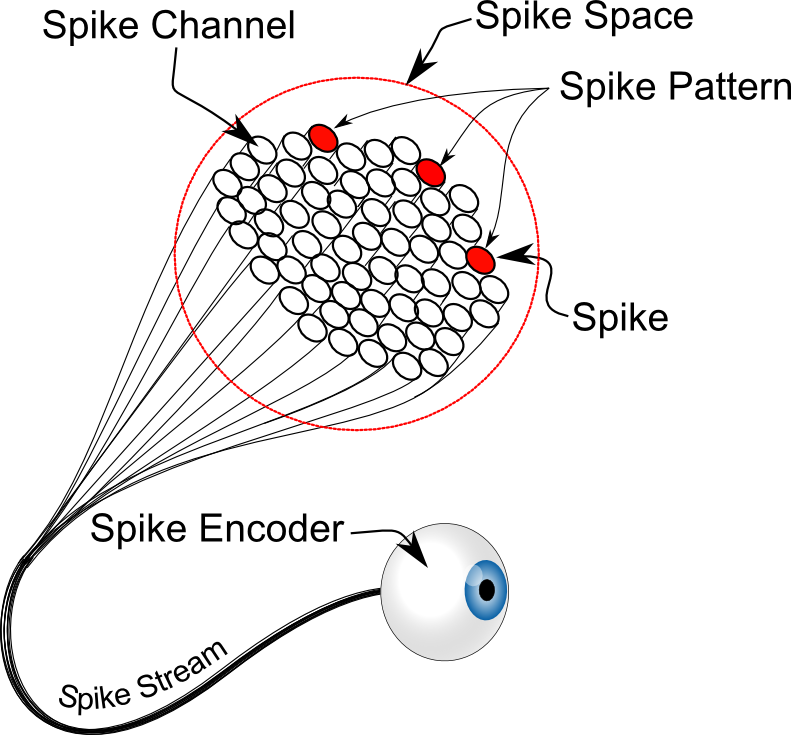
Spike Encoders (eye), Streams (wire bundle),Channel (wire), Space (# of wires), Pattern (active channels) and Spikes (the state of being active)
While there are many ways to encode information as spikes, it needs to be said that information in modern digital life is already spike-coded, we just don’t call it that. For example, the ASCII code maps integers in a 256 spike space to characters. We could use this code directly as a spike code. For example, the word “word” translates to the spike pattern: [119,111,114,100]. Digital images are already spike-coded as well. Each pixel in a 256 R-G-B encoded image, for example, gives us a spike pattern of length 3 (for the red, green and blue components) in a spike space of 768 (256×3). Directly using this spike code may not be a wise choice for other reasons, but its a spike code non-the-less. In general, if you map states or combination of states to discrete integers, then you are creating a spike code. The code does not have to be sparse, but there are advantages to sparse representation.
A wonderful thing about spike encoding is that it is really efficient, owing to the fact that we can get rid of the multiplication and only sum up the synapses that are spiking:

, where we use the convention that 
If you are thinking “man, using a bundle of N wires to transmit spikes over a spike space of N is NOT efficient”, we would say “agreed”. But then we would say “we do not actually do that”. We just communicate the spikes (integers) over a digital bus, which is how modern computers already encode and transmit information. This is much more “natural” than trying to map continuous mathematics, as is done with vanilla “continuous” neural network algorithms. I have little doubt the constraints of physics will push state-of-the-art machine learning algorithms toward discrete communication and low precision weights. In many ways, it already has.
Spike Streams Index Synapses
When you settle on a spike representation, the mapping to scalable “memory-like” architecture becomes fairly easy to grasp. A neuron is a collection of N differential pair memristor synapses. A spike stream generates spike patterns, where each spike is an integer in the spike space. If the spike space is equal to the size of the neuron, then the spikes in the spike pattern directly index the synapses of the neuron. This simplifies hardware design and can reduce or eliminate memory usage we would have to allocate to “address tables”, where a neuron ID goes in and the address of the synapses comes out. Synaptic computing becomes the procedure of turning on or “activating” different subsets of synapses at different time steps.
To make this easier to understand, take a look at a hypothetical kT-RAM core. Suppose we had a tiny core of size 64. To compute the neuron activation of spike pattern ![x=[0,6]](https://s0.wp.com/latex.php?latex=x%3D%5B0%2C6%5D+&bg=ffffff&fg=000000&s=0 "x=[0,6]")
READ instruction:
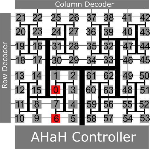
A 64 synapse kT-RAM Core, with synapses 0 and 6 activated
Just so the hard-core (pun intended) hardware folks do not get upset, we are not being totally honest here. Because a core can be “multiplexed”, numerous smaller neurons could exist on the same core. In this case, each AHaH node allocated to the core would have a partition index, and the actual address of the synapse to be activated is the partition index plus the spike id. It’s not much different than a random access memory, and that’s really the point. Information and communication is digital, while analog synaptic weights are stored, read and modified “on location” without having to transmit their state. Voltages are low. Activity is sparse. Weights are stored as analog values in novel memristor memory.
One last thing before I get back to crossbars. Many folks at this point ask me to explain the larger neural architecture or learning algorithm. This is like asking somebody who builds SRAM to explain their larger computing architecture, which of course makes no sense. kT-RAM is a building block, like SRAM is a building block. It can be used in many architectures. Its purpose is to provide a synaptic integration and learning resource. That’s it! You could form a specific topology of dedicated kT-RAM cores running hard-coded kT-RAM routines, or you could build very large general purpose cores that pair with CPU’s and run any routine you can dream up. The learning algorithm is not fixed–there are a universe of learning algorithms possible, constrained only by the kT-RAM instruction set. I use the Knowm API, our in-house simulation tool, to develop and test algorithms based on kT-RAM instruction set calls.
Non-Topological kT-RAM from Arrays of Memristor Crossbar Arrays
Consider a small “unit” crossbar formed of row and column bi-directional (pass-though) analog multiplexers and a small crossbar, as in the figure below. We will call this a “unit crossbar”.

A Unit Crossbar
A unit crossbar allows access to one of the NxM memristors in the array at any given time, where N is the number of columns and M is the number of rows. If the active column is specified on bit-lines “Sel-C”, the active row is specified on the bit lines “Sel-R”, and the enable input is low (or high, but let’s say low), then the addressed memristor in the array will see the full voltage applied to the SS (“source”) and DD (“drain”) lines. Lets re-draw this all as a symbol, as shown in “B” above. If we use, for example, an 8×8 unit crossbar then this circuit gives us access to one of 64 memristors, or none, at any given time. Seen in isolation, a unit crossbar is only capable of storing and retrieving single analog values. Not totally useless, but not very interesting either. As the name “Unit Crossbar” might hint at, however, the bigger idea is to form larger architectures from the base unit. So lets do this and recover a crossbar:

Crossbar formed of unit crossbars
Each unit crossbar exposes address bits 


Meta crossbar formed of unit crossbars
In this manner we have created a more ideal “meta crossbar” where elements can be isolated from the active row and columns in a similar manner to a selector device. However, because each memristor element of the crossbar is formed from a unit crossbar, we have actually created N distinct larger crossbars which are selectable by the select bit lines (S). While it may at first appear that using unit crossbars is overly costly, it is in fact a reasonable strategy when considered in the context of larger accelerators or networks, for example a deep neural network with dozens or even hundreds of layers. In this context, a single meta array could handle the whole network, or multiple networks for multiple applications, each selectable via the selection bits (S).
Wait, but didn’t I just say I don’t want to tie my hands with a set topology? While we could make this “meta crossbar” very large, due to the fact that sneak-paths within the larger array can be mitigated, I would really like a general-purpose array more appropriate to non-topological kT-RAM. If we replace the NAND row/column selection with a memory bit, and join all the columns together and all the rows together, we could get a non-topological kT-RAM half-core:
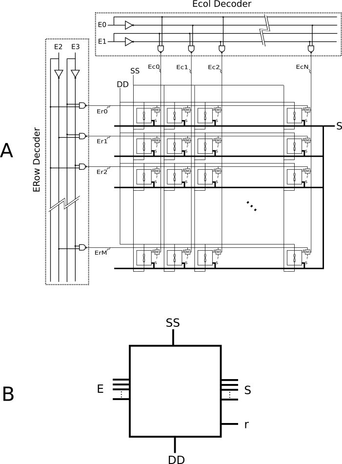
Non-topological kT-RAM half-core formed of unit crosbars
I say “half core” because a memristor synapse is formed from a differential pair. The differential is required to represent synaptic state (positive and negative), reduce common-mode noise including memristor decay, among some other things. There are many ways to form a differential pair, and while there are some arguments to be made for keeping the pair close to each other on a die, from a big picture perspective, it does not matter all that much where they are.
A quick clarification about the above diagrams before moving on. The row and column decoders are obviously not formed of arrays of 2-input NAND gates. Rather, each NAND gate must have 

The Need for an Intermediate Memristor Development Platform
There is a chicken-egg problem when developing memristor-based synaptic processors, if you are not interested in burning money. Before a chip can be built that is truly useful, you should convincingly solve real-world benchmarks to prove its primary (algorithmic) performance. However, developing robust algorithms for memristor synaptic processors requires access to memristor synaptic processors. Relying solely on simulation is risky, as I am not aware of any memristor model nor circuit simulation engine that fully captures the complexity of real-world memristors embedded in realistic circuits while allowing the simulation of reasonably sized networks on reasonably sized computers in reasonable time. Simply solving the MNIST benchmark, which is fairly trivial from a machine learning perspective, could takes weeks of simulation time! Worse yet, the result is likely dubious due memristor simulation complexities. It would be nice if somebody would build an intermediate platform that would give others easy access to at least a few thousand memristor synapses to support small scale demonstrations. Rather than develop algorithms that are supported only by simulation, algorithms could be developed live on a real memristor platform. The simulation time and complexity problem is side-stepped, and the result is guaranteed to work with real memristors because, well, it already is working with real memristors.
Relying solely on simulation is risky, as I am not aware of any memristor model nor circuit simulation engine that fully captures the complexity of real-world memristors embedded in realistic circuits while allowing the simulation of reasonably sized networks on reasonably sized computers in reasonable time.
When this intermediate platform is built, a whole new group of non-hardware folks could come on board. A server architecture would mean anybody in the world with interest, a computer and an internet connection could take part in algorithm discovery. When algorithms are demonstrated to be robust and useful, a fully integrated chip (or more likely many chips) could be built at dramatically reduced risk to all parties involved. To do such a thing, one would need access to a bunch of memristor crossbar chips, a few specialized tools, some basic electronics and programming skills and a lot of time. As luck would have it, since the great COVID-19 lock down, I had almost everything I needed!
Acquiring Tools and Space
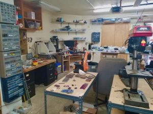
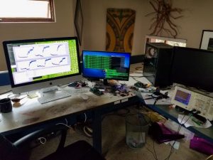
Before COVID I had already started to consolidate key pieces of equipment in my home. With the COVID-19 pandemic, I had the cover I needed to go off the deep end. Since COVID means I no longer have any guests stay at my house, the guest room found a new purpose. I installed a wrap-around anti-static workbench, an ultrasonic aluminum wedge wirebonder, a microscope, a UV and heat epoxy cure station and a smattering of other tools. In addition to my garage (the “dirty lab”) and office (the “computer lab”), I now have a clean lab! An unanticipated bonus revealed itself as allergy season hit. Having a clean lab with HEPA filters running 24/7 provides a much needed respite against the waves of grass and juniper pollen that drown northern New Mexico regularly.
| Clean Lab (former guest room) | Dirty Lab (former garage) | Computer Lab/Office (former den) |
|---|---|---|
 |
 |
 |
As software goes, I used the open-source and free KiCad EDA software for PCB design, as well as OSH Park for PCB fabrication and OSH Stencils for SMT stencils. For anyone not already familiar, I highly recommend the KiCAD EDA/OSH Park/OSH Stencils combination for PCB development. For simulating the pulse sense circuitry I used LTSpice.
With the COVID-19 pandemic, I had all the cover I needed to go off the deep end. Since COVID-19 means I no longer have any guests stay at my house anyway, the guest room needed a new purpose. I installed a wrap-around anti-static workbench, an ultrasonic aluminum wedge wirebonder, a microscope, a UV and heat epoxy cure station and a smattering of other tools.
Crossbars as Easy as Raspberry Pi
While the Analog Discovery 2 served us well for a number of years, this project called for something else. I did not need arbitrary waveform generators nor oscilloscopes and I would need much more GPIO. The popularity of the Raspberry Pi single board computer paired with high quality open-source and familiar Java API’s, led me to choose Raspberry Pi as a base platform. In addition to the host computer, building a kT-RAM array from unit-crossbars required a few additional modules.
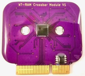
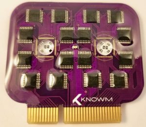
Crossbar Modules
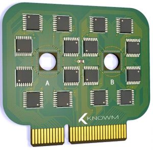
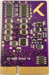
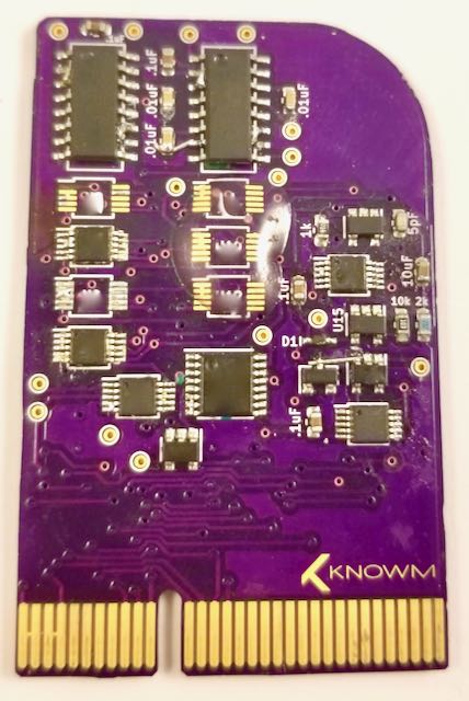
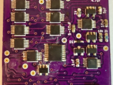
The crossbar modules used sixteen analog 8×1 multiplexers, one GPIO expansion chip, and one EEPROM chip for chip identification. I wire-bonded knowm crossbars directly to the PCB module with the least expensive aluminum wedge wirebonder I could buy, a vintage left-handed unit from China. Knowm crossbars come in a number of sizes, so with 8x8x4 dies and 8×1 multiplexers I can obtain four unit crossbars per die, and eight unit crossbars per module. The number of address lines also worked out well for the GPIO expansion chip, which is why I went with two die per module. Sixteen 8×1 multiplexers with three address lines each equals the 48 GPIO lines from the expansion GPIO chip located on the backside of the module. Based on earlier experience gained with Memristor Discovery, it’s important to use switches that have low charge injection, otherwise transient voltage spikes will wreak havoc on memristors during switch transitions. The simple act of turning a switch on or off could inadvertently cause voltage transients that will switch the memristor!
| 3D Render (front) | Fabricated (back) | Fabricated (front) |
|---|---|---|
 |
 |
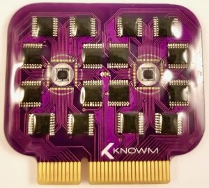 |
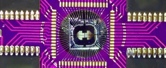
Close-up of one of the 4x4x8 crossbar die in the crossbar module
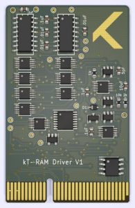
Pulse Driver & Sense Module
The unit crossbars need to be driven by low-voltage pulses and the current sensed. Based on experiments with Memristor Discovery, variable magnitude pulses of maximum +1V and minimum -2V would be needed, with accurate pulse widths in the range of 1-500 μs. Programmable bi-directional pulse generators are not terribly complicated to design, and I managed to fit three of them into about one square inch of 2-layer PCB.
The sense circuit was more complicated. The problem there was the relatively large mismatch between the Raspberry Pi GPIO timing, on the order of milliseconds with substantial error due to the fact that it’s software-controlled and subject to the whims of the thread schedular. The driver pulse generators are accurate to the nano-second and up to three orders of magnitude faster. When performing a read pulse operation, a small magnitude pulse of .2V or less is used to measure the (often only a few mV) voltage drop across a series resistor. My solution involved a circuit which is able to amplify the signal, capture the peak voltage drop across the series resistor and then store it as a charge on a capacitor long enough to be sampled by the relatively slow I2C analog to digital converter controlled by the Raspberry Pi. I spent a few hours on LTSpice testing various configurations that were relatively insensitive to component values.
| 3D Render (front) | Fabricated (Front) |
|---|---|
 |
 |
Main Board
The main board was the easiest component, simply a conduit between the Raspberry Pi host computer, the driver and crossbar modules. Two GPIO expansion chips are used for the mux enable lines across all six modules. Bridge connectors were used to help breakout the driver signal and also to join multiple boards together to form larger kT-RAM boards. I made one mistake, which is that I reversed the EEPROM I2C address lines. OSH park, the PCB fabricator, also failed to cut the board between the bridge connectors. I resolved this easily with a Dremel tool.
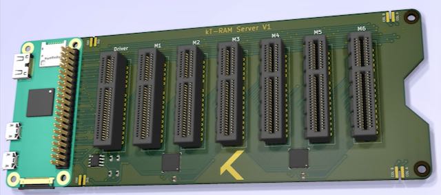
3D Rending of kT-RAM Server Main Board
Software
Software is usually the most time consuming aspect of projects like these, and this was no exception. The driver board required a number of SPI controlled chips, while the GPIO, analog to digital converter and EEPROM chips were run off of two I2C buses. I planned to use multiple crossbar variants, as well as upgrade the driver module and main board over time, so I included EEPROM identifier chips on everything, which of course needed to be programmed. Configuring the I2C GPIO expansion chips was exceptionally tedious, and my neck hurts just thinking about it. Each crossbar die has multiple crossbars, so I first needed to translate the relative-coordinate column/row address of each crossbar to absolute-coordinate column/rows. Next, given an absolute column and row indices I had to determine the specific multiplexer’s that control it. With that, I then needed to lookup the GPIO expansion chip on the main board and GPIO pins that controls the enable pins. But of course we are not done, because we still need to use the specified absolute column or row to find the mux channel that needs to be activated, and with the mux channel we need look up the bit pattern applied to the address lines, and with that we need to figure out what GPIO expansion pins control those so we can set them. Finally, we can set the GPIO–but not before reversing every 8 bits because, for some reason, thats just how its programed in the chip. Lookup tables aside, the rest of the code was simple. I wrapped everything up in a web-service exposing a number of end-points for configuring pulse generators, driving pulses and sensing, and moved to my desktop computer for testing.
Testing
Testing went fairly well. I was relieved to discover that the GPIO lookup tables were correct on first try. The pulse generators worked as expected, with the exception of some mis-wiring that I was able to fix with some PCB surgery and an update to the next PCB version. I stupidly forgot to purchase a sufficient quantity of a certain chip before testing, so I only populated the board with the bare minimum I had on hand and by-passed circuit elements I knew were OK with the wirebonder. The sense circuit also worked as expected, the one exception of a mis-wired element that I was luckily able to easily fix with an Xacto knife and micro soldering under the microscope. After testing I opted for a slightly larger capacitor in one location. I found that some I2C crosstalk from the A2D converter appeared in the driver sense pre-amp when the amplifier was dialed all the way up. However, due to how the sense circuit works and especially the timing, this noise is mitigated and did not appear to have adverse affects to circuit operation.
First test driver module with some PCB surgery to fix some dumb wiring mistakes.
In the second iteration of driver I found a 60mV bias that should not be there, which I fixed for the next generation driver. I failed to use a negative power rail for one key op-amp, resulting in a 60mV bias when it should be zero. I (frustratingly) took the negative supply out at the last minute in the first design to reduce circuit complexity, only to discover I actually did need it for just one of the amplifiers. I suspect i’ll lower the measurement noise with the fix as well. Thankfully the 60mV bias did not affect operations much except to make memristor erases touchy. Probably the dummest mistake occurred with the EEPROM chips, where I reversed the address bits on the main board. I was able to mostly fix this in software for testing, although it took me awhile to find the problem because the two module slots I randomly chose to use for initial testing, 1 and 6, had symmetrical bit address so they did not have a problem!
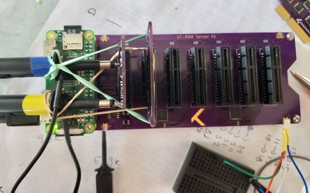
Testing the driver sense circuitry using the sophisticated “rubber band method”.
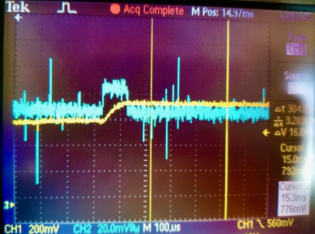
The driver sense circuit in action. The voltage peak across series resistor (blue trace) is captured by the sense circuit and held on a capacitor (yellow trace) until sampled by the A2D. Note the voltage scales and noise. Noise will be reduced with next driver versions.
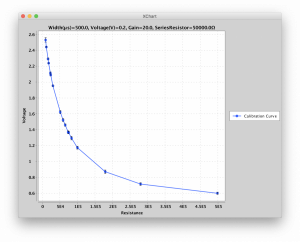
Probably the most important observation in testing was that I would need a dedicated calibration module. While it was not hard to derive the theoretical equation that mapped the sense read voltage to the sense current, component variations and parasitic capacitance skewed the ideal curve considerably, especially in the low-current regime, which would have made measurements way less accurate than I am comfortable with. To resolve this I made a dedicated calibration module with fixed resistors at known row/column addresses. By selecting sub-sets of the resistors I was able to produce a calibration curve from ~1kΩ to 499kΩ. To obtain a resistance I use the calibration curve to map the measured voltage to the resistance, interpolating between my calibration readings. This solution has one drawback: I must use the same read-pulse settings as was used for calibration, i.e., signal amplification, read pulse magnitude and width, and series resistance. However, since I try to keep all settings fixed when performing read operations anyway, this is not much of an issue.
| Calibration Module (front) | Typical Calibration Curve |
|---|---|
 |
 |
Once I began to test the crossbars it became clear that operating them in the 100kΩ-500kΩ was working out well. Due to the choice of leaving all non-selected rows and columns floating, the crossbars are sensitive to a stuck-on device or a device with a very low resistance. The memristors start out in a high resistance state (GΩ), and can be operated without elevated forming voltages in the 100kΩ-1MΩ range. Minimal current results in less wear and tear, higher endurance, and lower power. The only major drawback is that measurements are noisier. I thankfully included a programmable gain amplifier and programmable series resistor in the driver design, which allowed me to take measurements in the low current regime. While the noise is higher than id like, it’s workable and I have yet to employ any strategies to reduce it including differential synapses, which is the next planned step after the driver and sense circuits are tested and optimized.
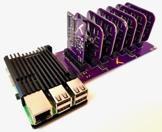
Completed Platform
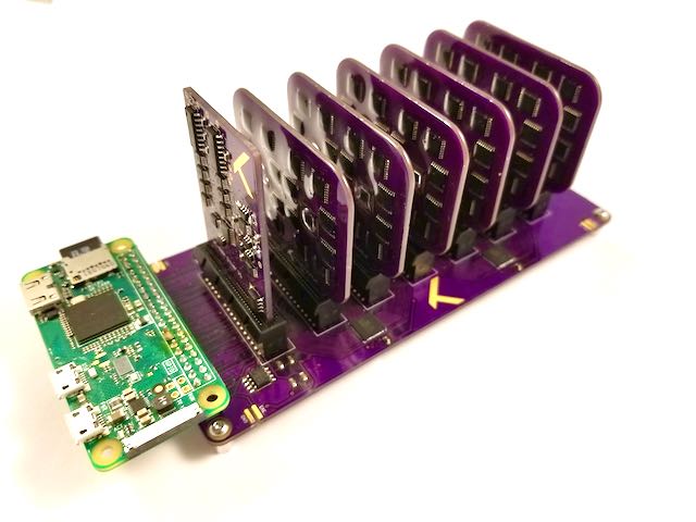
While I initially designed the board with the Raspberry Pi Zero W in mind, I couldn’t get over the horrible color clashing with the green Pi board. It looked unfinished with the poor little Pi Zero just dangling off the end, and all things considered there was no reason for such a small IoT computer driving everything. I grabbed a Raspberry Pi 3B+ with a black metal case I had lying around, soldered the mainboard to the bottom of the Pi board and sandwiched the two boards together with the metal case. The result looked much better to me and provided a dedicated ethernet port, something that seems like an obvious requirement of a “server” in retrospect! The only downside to this configuration is that I cannot join multiple boards together. I guess when that times comes I’ll just put them on a shelf in a dark room where I don’t have to look at them–the benefits of a server!
kTRAM Server With Raspberry Pi Zero. That green hurts the eyes!
kTRAM Server With Raspberry Pi 3B+ and metal heat sink. Much better!
The main board accepts six crossbar modules, and each module contains two crossbar die. Each die, in turn, can have multiple crossbars. Due to the design choice of 8×1 multiplexers for the row and column decoders, different crossbar die will result in different specs. In general, we can trade spike space for spike pattern length. For example, if we use the 8x8x4 crossbar die then we can get a maximum pattern spike length of 48 with 3072 memristors. On the other hand, if we go for the 32×32 crossbar die, we have a max spike pattern length of 12 with 12,288 memristors. While I may not utilize the feature for awhile, I designed the board with bridge connector slots on the corners. This enables multiple boards to be joined together in an essentially unlimited fashion. More practically, at least for the moment, the bridge connectors enable me to break-out the drive pulses and view on my oscilloscope.
Playing Around with Memristors
This project has been a great success as evidence by the fact I have had a hard time putting it down to write this blog article. As Richard Feynman said “There is a computer disease that anybody who works with computers knows about. It’s a very serious disease and it interferes completely with the work. The trouble with computers is that you ‘play’ with them!” I understand what he is talking about! When you have such easy access to thousands of memristors you can easily fall victim to the “What if do this!? What if I do that!?” disease. Worse yet, the complexity of memristors keep it interesting for hours. I promise to follow up with some more scientific results detailing my progress in the near future. Until then, here are some quick snap shots of what I have done in the few days after getting everything dialed in.
As Richard Feynman said “There is a computer disease that anybody who works with computers knows about. It’s a very serious disease and it interferes completely with the work. The trouble with computers is that you ‘play’ with them!”
In the plot below is a virgin memristor being driven by an n-write, n-erase repeating pulse sequence. The memristor starts in a high resistance state (>1MΩ) but moves down into an equilibrium range between ~220kΩ and 460kΩ. Note that this equilibrium range is a function of the write and erase pulses and series resistor and is not intrinsic to the device itself. Increasing the write voltage or decreasing the series resistor will lower the low-resistance state. Knowm M+SDC memristor can operate over large resistance ranges if you are careful, from kΩ all the way to 1MΩ! It’s the circuit they are embedded in and the voltages/currents applied to them that determine the realized resistance switching range.
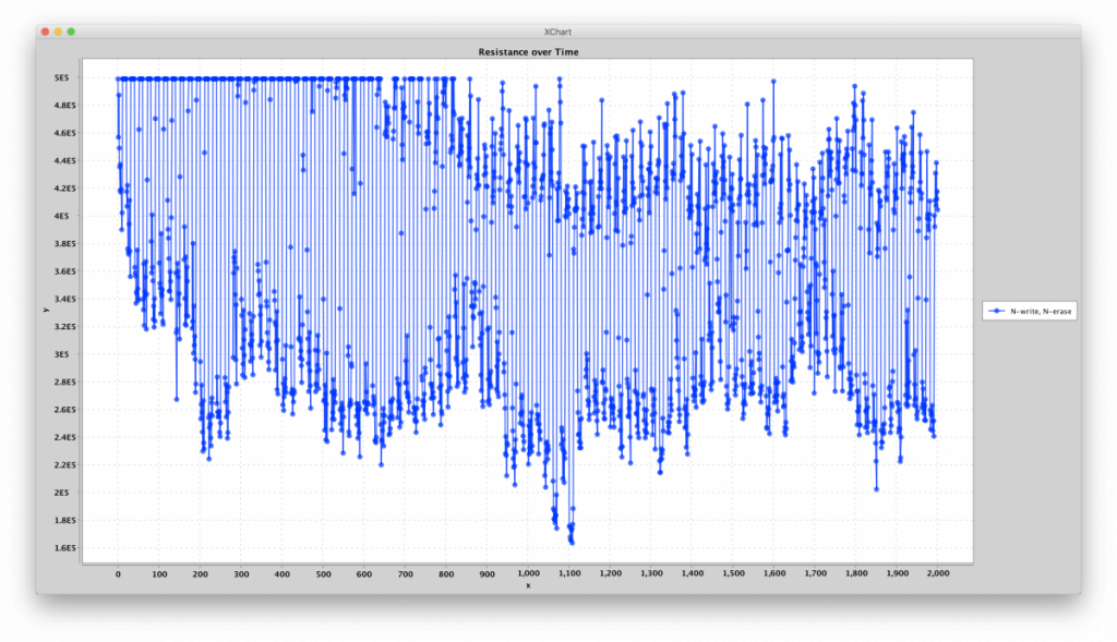
Evolution of resistance under a repeating 10-write (.4V I think), 10-erase pulse (.3V I think) sequence.
One of the first things I did, after demonstrating incrementing resistance states, was to work on algorithms for programming resistances. I came up with a relatively simple algorithm that would settle the memristor into the desired resistance, lowering the pulse-width as the measured resistance got closer to the desired resistance. (Specifically, the pulse width was chosen to be, in microseconds, the difference in resistance between the measured state and the target state, in kilo-Ohms.) I called it the “Flip-Flop” algorithm. It took anywhere from 2 to 100 pulses to nudge the resistance to within about 5kΩ of the target resistance. The limiting factor appears to be measurement noise due to the high resistances states. It’s going to be fun repeating this with differential pairs!
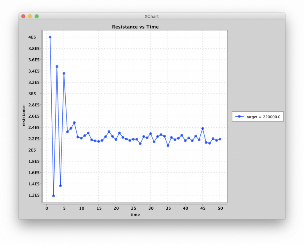
Programming resistance to 220kΩ via Flip-Flop algorithm
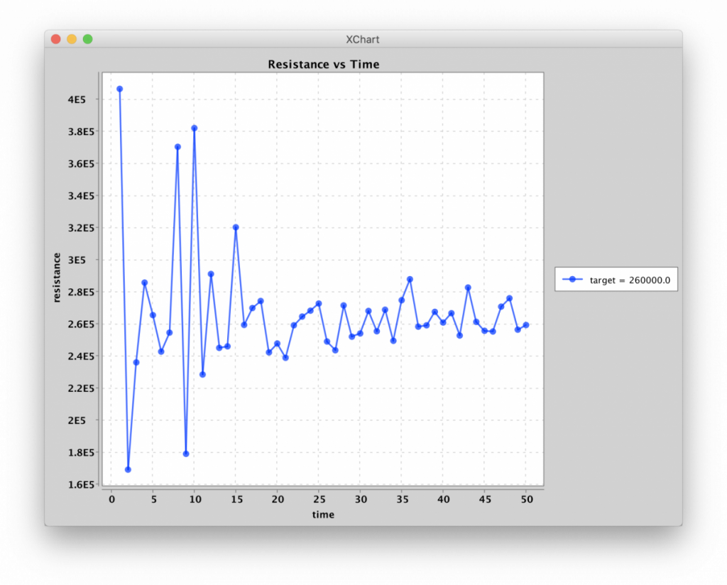
Programming resistance to 260kΩ via Flip-Flop algorithm
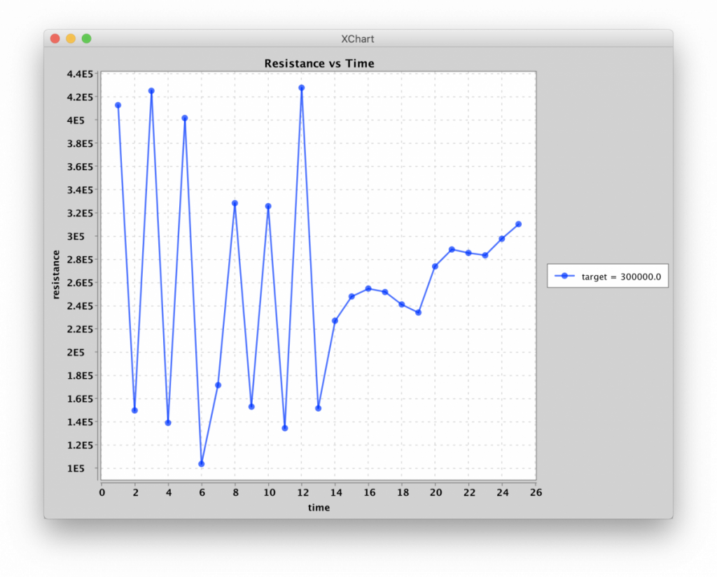
Programming resistance to 300kΩ via Flip-Flop algorithm
Due to the series resistor, which was set to 50kΩ for most of these experiments, driving the memristor into lower resistance states required quite a bit of pulse-pounding. This is because as the memristor resistance goes down, the voltage drop across it also goes down, which limits the force that can be applied. While this can obviously be overcome by increasing the applied voltage, it does illustrate the incremental nature of the devices at low applied voltages:
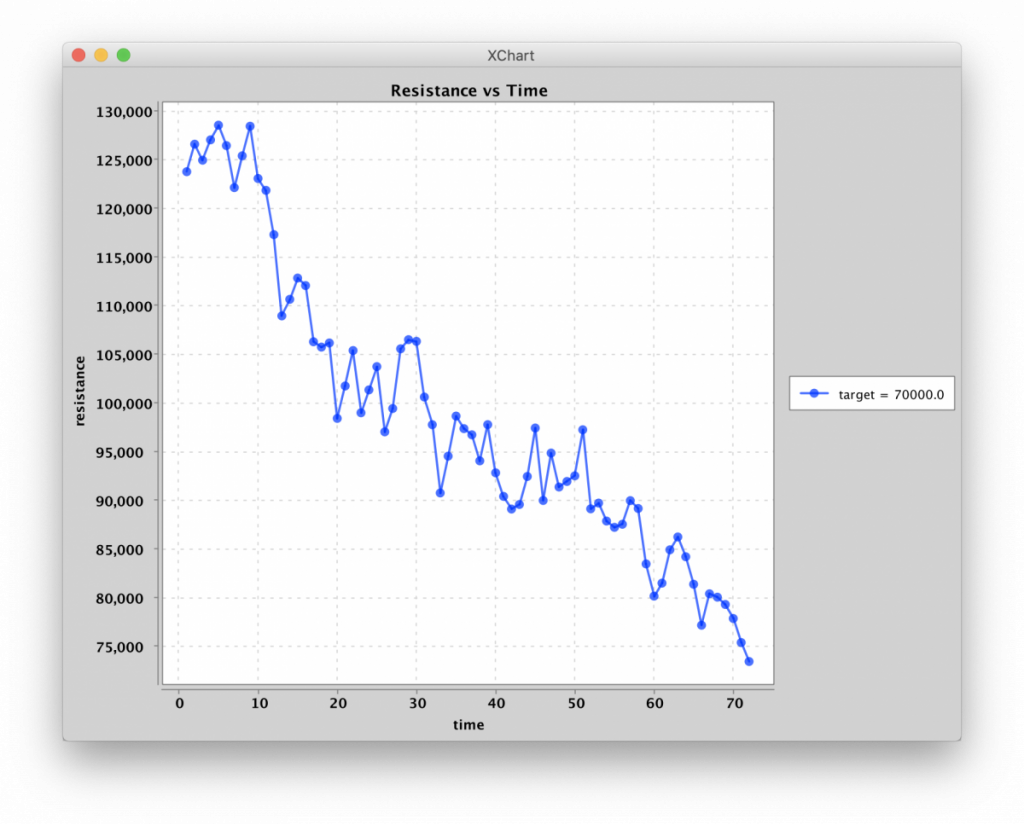
Programming resistance to 70kΩ via Flip-Flop algorithm
With programming of individual memristors under my belt, I moved to one column of an 8X8 crossbar. The challenge here is to write the resistance states of elements without disturbing the results of others. While I found it fairly easy to accomplish this across the rows of a column, I have not yet achieved perfect isolation when programming across a whole crossbar. Once I fix the 60mV pulse driver bias issue, I’ll re-visit the issue. The new boards and components for the updated driver module have arrived and all I need to do is stop writing this blog!
Resistance programming of one column of an 8X8 crossbar
At this point it was more or less obligatory to write a Knowm logo into the memristor array. I started with an 8X8 crossbar, which I was using for initial testing, so its lower resolution than I like. Not bad for a first attempt! Time evolution is from right to left:
Knowm logo being written to an 8X8 memristor crossbar
Not satisfied with the 8×8 resolution of the Knowm logo, I moved up to a 16×16 crossbar and attempted to program the logo again. This time I merged the images over time into an animated gif and gave it some (fabulous) color!

Knowm Logo in 16×16 Memristor Crossbar. Black(400kΩ) to Green(100kΩ)
It’s clear I still have some work with programming devices in isolation across the array, as evidenced most clearly by the annoying element in the (col=2, row=3) position, which should be in the high resistance state. Fixing the 60mV bias should help with this. All things considered, it’s nice to see 100% device yield across the array after multiple years on the shelf.
Final Thoughts and Next Steps
Programming the devices with the “Flip-Flop” algorithm reinforces to me that memristors are a viable path to ultra-low-power online learning. Increased positive bias and pulse width will increase conductance in increasing amounts, and visa-versa for negative voltage bias and pulse widths. However, conductance changes are not purely deterministic. While there exists an amazing continuum of resistance states and it is possible to accurately tune a device to a target resistance, the process looks almost exactly like learning and not much like programming. (There is an exception to this in regards to current-compliance programming, but I’ll save that for a future blog and perhaps driver module).
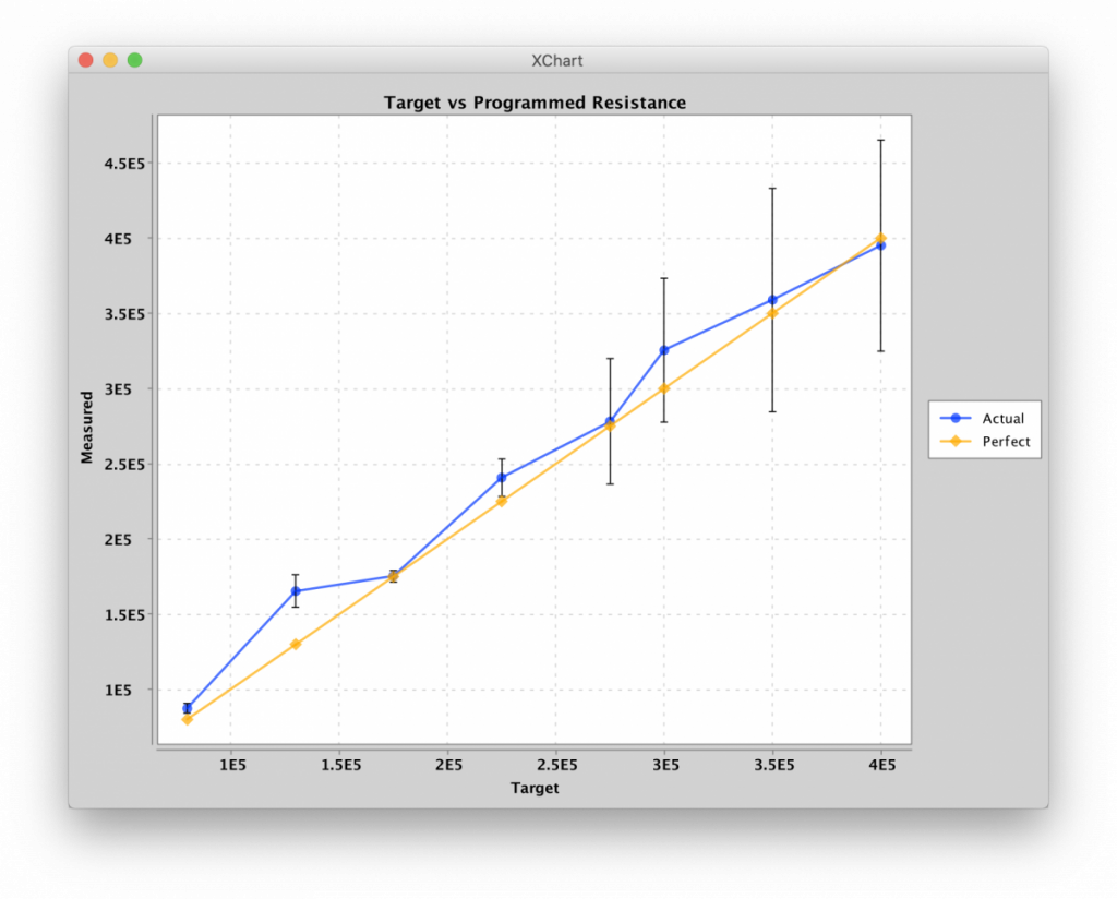
To illustrate the stochastic nature of the devices, here is some data I took over 10,000 trials where I start with a reset device (10 pulses, 500us width, -.3V amplitude) and then randomly write the device with a fixed voltage but variable pulse width. While it’s clear that wider pulses result in larger resistance changes, and it’s also clear that we have considerable measurement noise, it’s obvious that the conductance change is stochastic. This is not true for all voltages and pulse widths. As the voltage applied gets larger the transitions become more deterministic but also more binary, a property I had anticipated a long time ago with the generalized metastable switch memristor model.
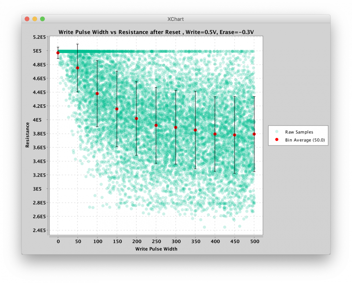
Memristor Resistance vs Pulse Width after Reset
While I dare to say this project has become fun, it’s true purpose is two-fold: (1) provide a real-time, real-memristor platform for kT-RAM algorithm design and verification and (2) provide the basis for a shared cloud-access memristor research server. I am looking forward to implementing the supervised classifier, unsupervised basis encoders and a number of other algorithms I developed on the simulator over the last few years, including some recent work with deep neural networks. I am also looking forward to opening up access to others around the world who share my passion so that we can all learn together. Stay tuned!
We’re not done yet! Check out Part 2.
Does this stuff interest you? Subscribe to our newsletter for updates.


10 Comments
Guarrera
Great blog Alex!
We are working on current compliance & noise reduction on Knomw devices.
We ‘ll share our result in near future.
In the mean time, I would propose you usage of FPGA as next step of your idea.
We can maybe found a collaborative approach around that ?
Regards
JP
Alex Nugent
Thank you, the project has actually been a lot of fun. FPGA is a great idea, especially to get around the GPIO timing bottleneck on the RPi. I do not have much experience with FPGA but would love to get some. We are certainly interested in collaborations!
Aliyu Isah
Hi Alex,
Thank you for sharing.
Regards
Aliyu
Franz Bruckhoff
Great work! Happy to see you‘re still on the ball and moving the field forward.
Hongyu An
where could I buy this product?
Alex Nugent
Hongyu–we are currently preparing it for beta product release, both as a web-service and also as a stand-alone platform. When it is available on our web-store (http://knowm.com/) we will announce it on our newsletter (https://knowm.org/knowm-newsletter/).
JP Guarrera
FlipFlop Algo looks nice. I guess for programming 220K or 260K your initial pulse width is different , isn\’t it ?(Because both take 50pulses to reach the targeted value)
Or maybe a voltage difference ? Thanks in advance for your comment.
Alex Nugent
Devices are stochastic. Same pulse applied on the same memristor starting from the same resistance value can lead to different results. You can affect the probability (higher voltages and pulse widths are more likely to cause larger changes). Sorry for late response, this comment was caught in spam folder and I only saw it now.
edit: also in the case of 50 pulses, thats just when I stopped recording. It takes a variable amount of pulses to achieve target, and then I just let it ran without programming after that.
Shubham Paul
Hi Alex,
Impressive and very well made article. I have a small question though, you have mentioned that you are using \’unit crossbars\’ and using a 2D array of \’unit crossbars to reduce sneak path currents but how are you reducing sneak path currents inside a single \’unit crossbar\’?
I mean when using an analog multiplexer to select a single memristor in a unit crossbar to read/write, won\’t the sneak path currents due to nearby memristors (in the same unit crossbar) cause issues in reading and writing the selected memristor? I would very much like to know about this.
Regards,
Shubham
Alex Nugent
Shubham,
Sorry the comment was caught in our spam filter (it said cookie not set). I am suggesting one work with the sneak path by keeping crossbars small and just factoring that into your use. You cannot eliminate it unless you use selector devices or drive the whole crossbar. By keeping crossbars small you can reduce effects, so in this case that is what I am doing. Sneak path is still there but its not debilitating.