I recently came across a discussion thread on Y Combinator Hacker News, which has been archived here. After looking into the law regarding defamation of character and taking a few deep breaths–I decided it would be better to offer a public response.

Context
The discussion thread occurred toward the end of July in response to the announcement by Wei Lu’s group of their “First Programmable Memristor Computer”. Perhaps related, perhaps not, one week before this discussion we received an odd communication via our website contact form:
From: Jonathan Wardle jonwardle7@gmail.com
Subject: Are you legit?
Message Body:
I am a hobbyist and maker who is intrigued by your product. However, I remain somewhat unconvinced that your company is not some sort of scam. Can we resolve this in a way that is mutually beneficial?
—
This e-mail was sent from a contact form on Knowm.org (http://knowm.org)
I found this email intriguing, don’t you? Knowm is not a scam, and that’s that. If Mr. Wardle wants to convince himself of that he can purchase our low cost memristor discovery kit on the webstore and start researching with our Memristors today. He can do this because we are the only company (so far) that will let anybody actually probe and test their memristors.
I have been working on memristor neural networks since January of 2002, when I first asked my physics professor to sign an inventor disclosure notebook. For the first fourteen or so years the hardest part was the technical challenge and acquiring the resources to meet it. We were completely focused on achieving proof-of-concept and engaging with and working with any person or organization that was willing to help. Venture capital or public research funding for novel hardware, especially for small business, was non-existent in those years. We knew the project would require a huge investment in research, so beyond small initial friend-and-family investments, we made progress thanks to Air Force Research Labs and Office of Naval Research. Crossing the technology stack from atoms to AI has been the most difficult and personally rewarding aspect of my adult life. Over the last two years the exploding field has become riddled with politics and intellectual property posturing. If that is not a sign that a technology is maturing I don’t know what is.
Defamatory Y Combinator Hacker News Thread
No sooner is a memristor mentioned as somebody points out the fact that you can buy some at knowm.org. This is where the fun begins.
This looks like a snake oil salesman rebranded CBRAM as a memristor and hoped nobody qualified would notice that they’re claiming a revolutionary breakthrough. –throwawaycert
This is interesting because we actually are claiming a breakthrough and we are absolutely qualified to make such claims. Our metal-doped Self-Directed-Channel devices (M+SDC) are an innovation that has resolved shortcomings of CBRAM devices in both device properties and device manufacturing. Both CBRAM and our M+SDC devices can be seen as sub-type of broader electrochemical metallization (ECM) memories:

Memristor Taxonomy
The CBRAM device changes resistance through a mechanism involving the formation and dissolution of a conductive filament between the top and bottom electrodes in response to a potential applied across the device [1]. The first chalcogenide CBRAM was developed at Arizona State University (ASU) by Kozicki. It was patented in 1998 [2,3] and assigned to Axon Technologies, who in turn licensed the technology to Micron Technology and others [4]. The technology proved difficult to manufacture, and was modified and improved over the years by several companies, including Micron [5,6].
The chalcogenide ion-conducting memristor went in a different technological direction with the invention of the SDC device [7-8]. This device uses a metal-chalcogenide layer between a specific type of chalcogenide with homopolar bonds on the non-chalcogen atoms (Ge2Se3 or similar), which removes the need to photodope the chalcogen with a mobile metal, such as Ag. The SDC device is not critically dependent on the amount of Ag doped into the glass layer since it does not require any photodoping [9], resulting in an easier to manufacture and more reliable device with thermal stability.
Innovating further on the SDC device, Dr. Campbell developed at Boise State University (BSU) a way to alter the device electrical properties by metal doping of a chalcogenide layer, and sandwiching that layer between two undoped layers. The type of metal that is doped in the chalcogenide layer determines the device electrical properties, including threshold switching voltages, resistance states achievable, resistance state retention, capacitance and charge storage, as well as the resistance change mechanism (i.e. phase change or ion conduction). Tunable device electrical parameters are critical to the development of analog applications of memristors such as neuromorphics. This innovation was patented in 2015, assigned to Boise State University, and licensed to Knowm Inc. [10,11].
No, they make a claim and their only sources are their own work that doesn’t appear to have been peer reviewed or even vouched for by anyone that doesn’t work for them. –throwawaycert
This is false. You can read about SDC devices in this peer-reviewed paper. If you like, here is a lecture. You can also read our peer-reviewed paper on AHaH Computing here. You could also do a literature search for Knowm memristors.
A true memristor as envisioned by Chua would be a revolutionary device of extreme utility. If knownm has what they say they have, the company would be worth billions. But they’ve been around for years and their website looks like every other scammy snake oil site out there. –throwawaycert
If you ask Leon Chua where you can buy a memristor, he will point you to us–as he does in his recent paper. We have exactly what we claim to have. We sell it on the webstore. We offer a low-cost platform that enables anybody to use the memristors. What other company will let anybody test their memristors? Seriously, name them. We make it possible for educators, students, and hackers around the world to actually gain hands-on experience with memristors, so that the theory can get grounded in reality and not hype.
Who are their process engineers? Where is their fab? Are they contracting with a third party? Who? Will they vouch for the technology? –throwawaycert
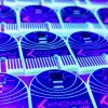
All Knowm wafers have been made by the device inventor, Dr. Kris Campbell, at the Idaho Microfabrication Laboratory at BSU. We previously contracted with third-party packagers but we have moved that in-house after discovering issues related to wirebonding aluminum wire to thin tungsten metal pads and had to develop our own successful packaging process. Hence our really cool looking new chips with audited 99.95% yield (2 wirebonds + device) and five year demonstrated shelf life. Here is a recent peer-reviewed open-access paper that explores our memristor:
By the way, you can buy Ioannis Vourkas’ textbook on memristors on amazon:

The “Memristor Discovery Platform” was made by… Knowm. (in other words, “it works because I say so”). –throwawaycert
There is no memristor that has been scrutinized and third-party validated more than ours for the relatively simple reason that we are the only company in the world that allows our memristors to be tested in isolation, i.e. not part of a larger integrated circuit such as a memory array, by anyone without NDAs or any other obnoxious agreements. We have sold our memristors to researchers and competitors in over forty countries.
…their documented staff are mostly dedicated to “intellectual property”. This is a scam and/or patent troll. End of story. –throwawaycert<
Just like every other technology company, we protect our ideas with patents. Patents are not an option, they are a requirement. If we were patent trolls our business model over the last five years would have been entirely different.
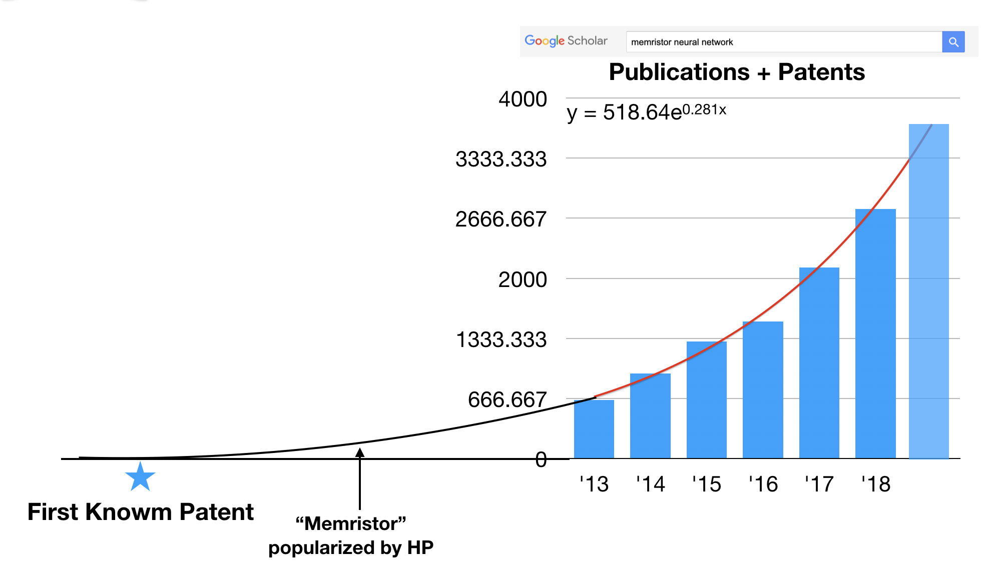
The first Knowm patent on memristive neural networks was filed in 2002. The field is currently exploding with interest.
I will wrap this up by quoting CodiePetersen, who thankfully came to our defense when the Y Combinator moderators did not.
Why don’t you just talk to them yourself instead of ranting on YCNews. It amazes me how many people don’t follow the guidelines on this site and the mods just let it fly. Every single one of the members of Knowm you can directly email. I know because I have actually talked to them. One lady is not on Linked in so you will have to talk to her through her her academic email.
On that note, please contact us if you have honest questions or need help with your Memristor Discovery kit. Happy hacking and beware the internet trolls.
References
- Valov, Ilia, et al. “Electrochemical metallization memories—fundamentals, applications, prospects.” Nanotechnology 22.25 (2011): 254003.
- Kozicki and West, US Patent 5,761,115 “Programmable metallization cell structure and method of making same.” June 2, 1998 [CBRAM original]
- Kozicki, M.N. US Patent 6,487,106 “Programmable microelectronic devices and method of forming and programming same.” November 26, 2002 [More CBRAM]
- “Micron Technology Licenses Axon’s Programmable Metallization Cell Technology..” The Free Library. 2002 Business Wire 28 Nov. 2016 https://www.thefreelibrary.com/Micron+Technology+Licenses+Axon%27s+Programmable+Metallization+Cell…-a081898511
- Campbell, Kristy A. and Moore, John T., US Patent 6,784,018 “Method of forming chalcogenide devices and method of forming a programmable memory cell of memory circuitry.” August 31, 2004 [More CBRAM, assigned to Micron Technology]
- Campbell, Kristy A., and Moore, John T., US Patent 7,067,348 “Method of forming a programmable memory cell and chalcogenide structure.” June 27, 2006 [More CBRAM, assigned to Micron Technology]
- Campbell, Kristy A., US Patent 7,030,405 “Method and apparatus for resistance variable material cells.” April 18, 2006 [SDC originals, assigned to Micron Technology: (Note: using Ag2Se as the metal-selenide layer)]
- Campbell, Kristy A. and Moore, John T., US Patent 7,151,273 “Silver-selenide/chalcogenide glass stack for resistance variable memory.” December 19, 2006 [SDC originals, assigned to Micron Technology: (Note: using SnSe as the metal-selenide layer)]
- Campbell, Kristy A. “Self-directed channel memristor for high temperature operation.” Microelectronics Journal 59C (2017) pp. 10-14. DOI 10.1016/j.mejo.2016.11.006. Full article can be accessed at: https://authors.elsevier.com/sd/article/S0026269216303779
- Campbell, Kristy A. US Patent 9,118,006 “Carbon-Chalcogenide Variable Resistance Memory Device.” August 25, 2015.
- Campbell, Kristy A. Patent Application No. 14/727,618 “Tunable variable resistance memory device.” [SDC tunable, assigned to Boise State University, Licensed by Knowm, Inc.]
1 Comment
Jacob R. Steeves
“If knowm has what they say they have, the company would be worth billions.”
Truly hilarious. You’ve reached the point where your company is so legit that people assume its a scam.