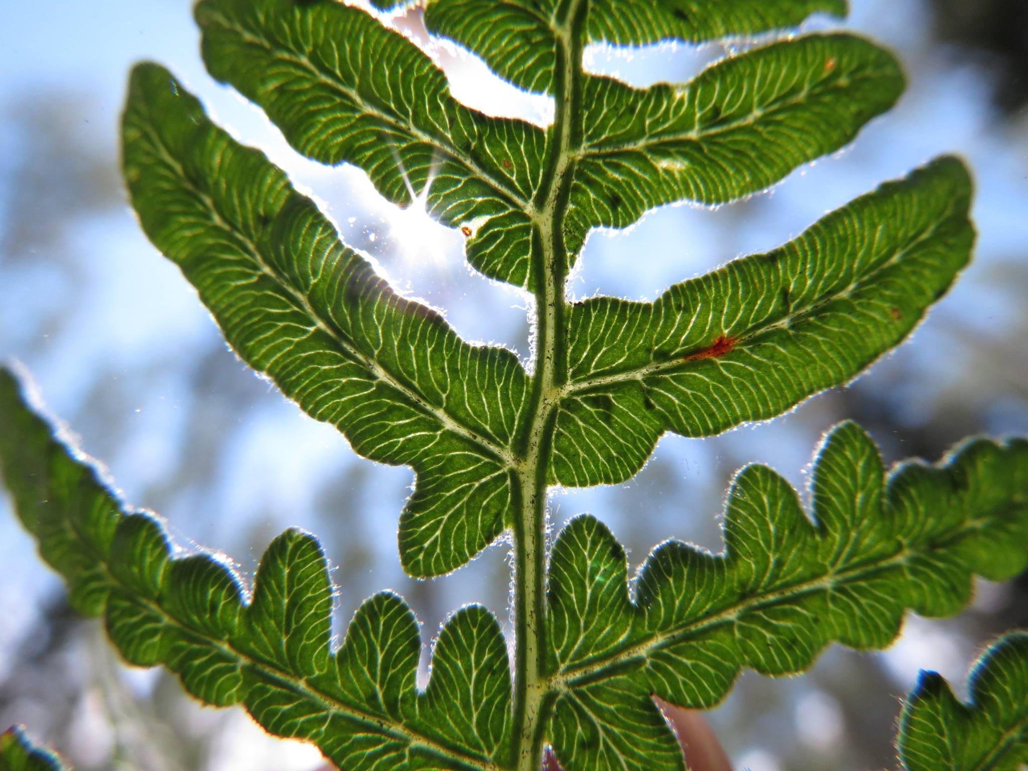
Looking Into Nature
The electron transport chain in photosystem II is one of the most important biochemical reaction pathways for life on this planet [1]. It starts with the absorption of a photon of light from the sun and through a sequential chain of several redox reactions, extracts energy that the photosynthesizing organism can use in a multitude of chemical reactions. These reactions keep it alive, form sugars, help it grow, reproduce, and ultimately generate oxygen molecules (O2) that are delivered to the air we breathe. It is the study of oxygen evolution and how the photosynthesizing organism (plants, Cyanobacteria) actually extracts electrons from water and forms O2 that stirred my interest in science.
In graduate school I was fortunate enough to be able to devote myself completely to the study of the chemical complex responsible for oxygen evolution (referred to as the Oxygen Evolving Complex – OEC)
Fractal Energy Flow
In graduate school I was fortunate enough to be able to devote myself completely to the study of the chemical complex responsible for oxygen evolution (referred to as the Oxygen Evolving Complex – OEC [2,3] at the University of California, Davis, under one of the world experts in this area, Dr. R. David Britt. By the time I received a PhD, we still did not know what the structure of this fascinating complex was, but we made remarkable strides towards elucidating the oxidation states (during the Kok cycle S-states [3]) of the four manganese atoms that comprise this structure. Since that time, X-ray crystallography has taken researchers even further towards understanding the structure of this elusive complex, but the structure is still unknown during each S-state cycle [4].
Understanding the Past
The study of the redox reactions that occur with the OEC led me naturally to the investigation of electronic devices that operate to change their resistance state based on redox reactions of a metal, such as silver or copper. These types of electronic devices are often referred to as “ion conductors” because an electric potential difference across the two terminals of the device can cause the metal to oxidize and become mobile within the device material, migrating from the higher potential oxidizing electrode to the lower potential reducing electrode. These types of devices become very interesting when one thinks about how to design a device material that can interact with this mobile metal ion in such as way so as to tune the electron transfer, ultimately leading to the ability to tune the electrical properties of the device.
Interestingly, one of the early devices that uses Ag ion-conduction to change device resistance was described by Hirose and Hirose in 1976 in which a thin film layer of the chalcogenide material As2S3 was photodoped with silver.
This concept of device tuning has a direct analogy with the OEC; it is the influence of adjacent atoms, amino acids, and proteins on the electron transfer events within this complex that influences the process of water oxidation and oxygen evolution [5]. Interestingly, one of the early devices that uses Ag ion-conduction to change device resistance was described by Hirose and Hirose in 1976 in which a thin film layer of the chalcogenide material As2S3 was photodoped (a process where light is used to drive redox reactions and to cause Ag ion migration and incorporation in the chalcogenide material – another photosynthetic analogy!) with silver to incorporate the silver throughout the film [6]. A potential was applied between two electrodes in contact with this photodoped chalcogenide and not only did the device resistance decrease by orders of magnitude, but optical observations showed the presence of silver dendrites in the chalcogenide film (the very large device was manufactured ‘horizontally’ so that the active material could be observed during application of the potential). It was the silver dendrites that created a conductive pathway between the electrodes – one that was reversible if the potential was reversed. This was one of the first non-volatile memory devices based on ion-conduction in photodoped chalcogenide materials. It was followed up later in the late 1990’s by the patenting of ion-conducting devices using photodoped chalcogenide materials (interestingly, also covering the device material system shown in 1976 by Hirose and Hirose) [7]. Modifications of the types of materials photodoped and the metals used during device operation ensued (more on this HUGE topic to come in a future discussion!).
Rethinking What’s Possible
The drawback with each of these photodoped device options is the removal of the ability to tune the material’s electron transfer properties. This major drawback led to rethinking how to make ion-conducting devices: how do we eliminate this photodoping process and the limitations imposed by selection of materials that can be photodoped, but still create a conductive pathway that we can better control? The elimination of photodoping started with materials layering which proved to be the starting point of materials tuning [8].
By thinking about the device from the perspective of how biological systems handle electron transfer, we’ve been creating devices that are more controllable in terms of operational parameters. These parameters include threshold voltages, resistance ranges, switching speeds, data retention, and cycling durability.
By thinking about the device from the perspective of how biological systems handle electron transfer, we’ve been creating devices that are more controllable in terms of operational parameters. These parameters include threshold voltages, resistance ranges, switching speeds, data retention, and cycling durability. It’s always an exciting day in the lab when wafers with devices comprised of the latest experimental film have completed fabrication and are ready for testing. There is an abundance of knowledge that is gained every time that first IV curve is measured – and it’s the new questions that arise with every experimental result that keep us driven to learn more!
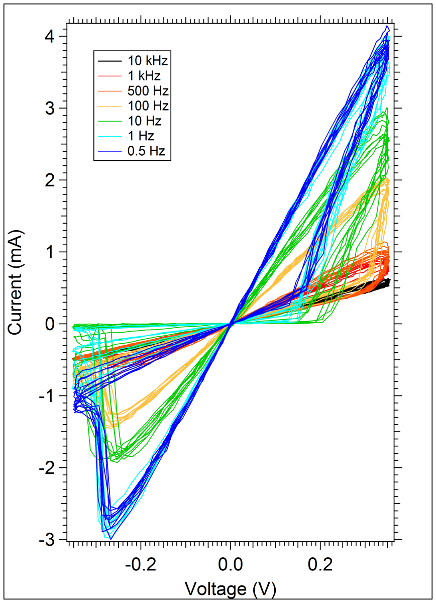
Knowm Memristor Frequency Response Fixed V amplitude
Collaboration with Knowm
Knowm has now been working together with Dr. Kris Campbell for over a year, and have thus far fabricated three new memristor types with ideal AHaH Computing properties and neuromorphic computing applications. Together, we have worked hard to develop and offer the world a commercially available discrete memritsor based on one of Dr. Campbell’s recent devices optimized for neuromemristive computing. Knowm hopes that making this new technology available to anyone will spark new collaborations and innovations across the world. The future is looking very exciting!
Related Resources
- Dr. Kris Campbell’s page on knowm.org: http://knowm.org/teams/kris-campbell/
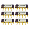
- Knowm’s Commercially Available memristors: http://knowm.org/product/bs-af-w-memristors/
- Knowm Collaborates with Kris Campbell at BSU: http://knowm.org/knowm-collaborates-with-kris-campbell-at-bsu/
- The Trouble with Oxide-based Memristors
- Articles Tagged with Kris Campbell
- SDC Memristor Development History
- The Constraints for Neuromorphic Computing Systems Have Suddenly Changed
- Knowm Inc.’s BS-AF-W Memristors
- How to Build the Ex-Machina Wetware Brain
- The Generalized Metastable Switch Memristor Model
References
- Rochaix, Jean-David. “Regulation of photosynthetic electron transport.” Biochimica et Biophysica Acta, Bioenergetics (2011), 1807, 375-383.
- Britt, R. David; Suess, Daniel L. M.; Stitch, Troy A. “An Mn(V)-oxo role in splitting water?” Proceedings of the National Academy of Science of the United States of America (2015), 112, 5265-5266.
- Hillier, Warwick; Messinger, Johannes. “Mechanism of photosynthetic oxygen production.” Advances in Photosynthesis and Respiration (2005), 22, 567-608.
- Davis, Katherine M.; Pushkar, Yulia N. “Structure of the oxygen evolving complex of photosystem II at room temperature.” Journal of Physical Chemistry B (2015), 119, 3492-3498.
- Debus, Richard J. “FTIR studies of metal ligands, networks of hydrogen bonds, and water molecules near the active site Mn4CaO5 cluster in photosystem II.” Biochimica et Biophysica Acta, Bioenergetics (2015), 1847, 19-34.
- Hirose, Y.; Hirose, H. “Polarity-dependent memory switching and behavior of Ag dendrite in Ag-photodoped amorphous As2S3 films.” J. Appl. Phys. (1976) 47, 2767-2772.
- Kozicki, Michael N.; West, William C. “Programmable metallization cell structure and method of making same.” US Patent 5,761,115, issued June 2, 1998.
- Campbell, Kristy A.; Moore, John T. “Silver-selenide/chalcogenide glass stack for resistance variable memory.” US Patent 7,151,273, issued December 19, 2006.


1 Comment
Knowm First to Deliver Configurable Artificial Neural Networks using Bi-Directional Learning Memristors | Chip Design
[…] Dr. Kris Campbell of Boise State University had been researching the electronic properties of chalcogenide […]