Oxide-based Memristors
I have been asked a number of times how the memristors I designed for Knowm Inc. differ from HP’s memristor. For every comment I make, I have to stress that I have not personally tested HP’s memristors. Their actual electrical properties could deviate from my own experience fabricating similar devices and from what I’ve read and heard from others. The problem with relying on second-hand reports is that the electrical properties of a memristor can be significantly altered by how the device was previously tested or handled. I don’t know how sensitive HP’s devices are or how easily they can be damaged. Sometimes one can observe erratic behavior due to previous mishandling of the device, so without knowing the exact history you can never be 100% sure. Given the above, my observations from similar devices that I have fabricated are congruent with what others, who have tested HP’s memristors, also claim.
Sometimes one can observe erratic behavior due to previous mishandling of the device, so without knowing the exact history you can never be 100% sure.
They have been described as erratic, with high switching voltages, high forming voltages, and non-repeatability from device-to-device. The published literature for HP’s devices claim it is comprised of a metal oxide material that relies on the migration of oxygen vacancies to alter the resistance of the device. This oxygen vacancy migration is related to the volume of the device active layer and is thus considered a ‘bulk’ migration, not necessarily a filament through the device.
They have been described as erratic, with high switching voltages, high forming voltages, and non-repeatability from device-to-device.
However, that being said, there are also patents (by other companies researching metal-oxide resistive RAM) that support the development of a device structure using oxygen vacancies that form a filamentary conduction path or percolation path (e.g., US8648418, US9012881B2,US20130341584A1). I do not know if HP is implementing any of these types of designs, or even perhaps something new. Other types of metal-oxide devices are described in the patent literature to address the erratic switching issues, and the high forming voltages (US8062918B2, US20140054531A1, US8441838). Even more patents address molecular control of the oxygen vacancies through material design and device structure (e.g., US8420478B2). There are hundreds of patents that address these issues, and what I reference above can serve to get anyone that is really interested in digging deeper a starting point

Image by darkday. 
The Trouble with Oxide-based Memristors
From my own experience with some of the metal-oxide devices, such as HfOx, I have found that oxides are very difficult to design a stable device with. First, it is very difficult to control the concentration of oxygen within a film. Fabrication techniques become complicated every step of the way. Keeping oxygen out of the device after fabrication is also challenging. I have first hand observed device-to-device variation in metal oxide devices that I’ve fabricated, with high switching voltages, erratic behavior within the same device, and poor state retention.
I have first hand observed device-to-device variation in metal oxide devices that I’ve fabricated, with high switching voltages, erratic behavior within the same device, and poor state retention.
My opinion is that it is difficult to fabricate devices with metal-oxides since it is difficult to control or regulate the concentration of oxygen in the device. This means that every time one tries to fabricate devices, they may get different results due to any small change in the way the wafers were processed. This is an exercise in frustration. Different film deposition methods will produce devices with drastically different electrical characteristics. I do not use oxides for this reason.
The Benefits of Oxide-based Memristors are Debatable
Benefits that I’ve heard attributed to oxide-based memristors include that they would be compatible with CMOS processing or that they can withstand higher temperatures during fabrication. I disagree with the compatibility analogy since the metals of the metal oxides may still pose a problem as a contaminant in a clean room, especially if the materials have been specially designed to address a particular problem. Compatibility can be addressed through circuit designs that place the memristor fabrication as a back-end-of-line (final) processing step. The higher processing temperatures could certainly be true, but through back-end-of-line processing, this isn’t an issue.

Image by JamesIrwin
More Reliable Memristor Devices Can Be Built
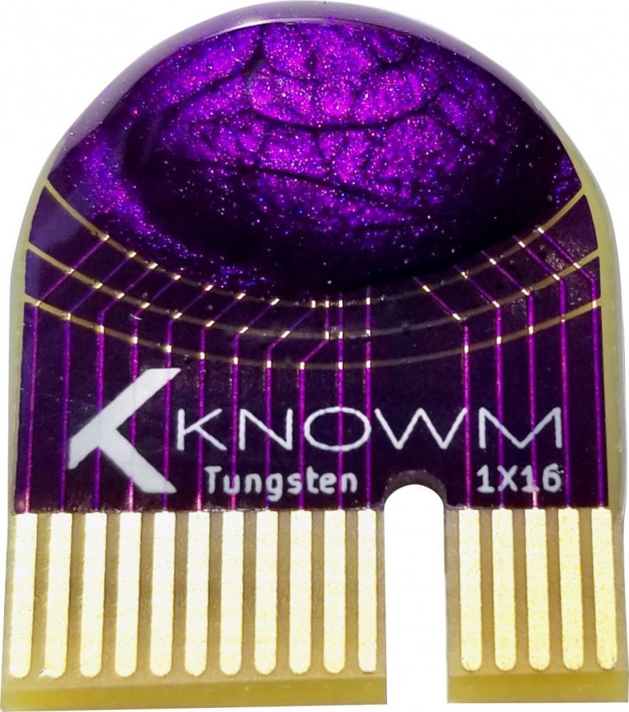
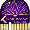
Knowm 1X16 Memristor Array Chip
Our devices do not use oxygen vacancy migration to change the device resistance. The Knowm memristor uses layers of chalcogenide materials. Due to the amorphous nature of the materials–meaning they are disordered and not affected by impurities due to Fermi level pinning [1], they can take on impurities such as oxygen with little to no observable effect on the electrical properties. The devices rely on both a phase-change and an ion conduction mechanism, with the ion conduction mechanism dominating during “normal” low-voltage operation. The active layers do not have a need for precise thicknesses and they can be deposited in a variety of ways, including the simple technique of sputtering. Even with fabrication in the university clean room where pieces of equipment are in constant flux, even with unexperienced undergraduate students fabricating the devices, they still behave with similar electrical properties every time. The switching voltages are low, the forming voltage is low, device switching is consistent, and fabrication is simple.
Read more: Self-directed channel memristor for high temperature operation
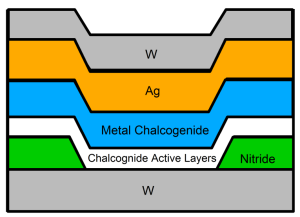
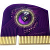
Knowm memristor material stack
- For a description of “Pinning of the Fermi Level” in amorphous chalcogenides, please see (for example) chapter 2.1.1 of http://link.springer.com/chapter/10.1007/978-3-642-28705-3_2?no-access=true. Some online material, like this, is only relevant in a crystalline semiconductor.
Further Reading
- Do Oxide Memristors Have Shelf-Life Issues?https://knowm.org/oxide-memristors-have-shelf-life-problems/
- Dr. Kris Campbell’s page on knowm.org: http://knowm.org/teams/kris-campbell/
- The Story of My Memristor – Kris Campbell http://knowm.org/the-story-of-my-memristor-kris-campbell/
- Knowm Collaborates with Kris Campbell at BSU: http://knowm.org/knowm-collaborates-with-kris-campbell-at-bsu/
- SDC Memristor Development History


Leave a Comment