[popupwfancybox id=”7″]
Omissions in Review Paper from University of Michigan
The field of memristors exploded over the last ten years, so it can be hard to keep everything straight–especially if you are not a physical chemist that specializes in memory materials. As Knowm moves from research and testing into active commercialization, we spent some time looking at memristor review articles. We were searching for a nice way to compare Knowm’s SDC memristors against other memristor types. This is hard to do with memristors because you can’t always trust the literature and it’s almost impossible to get devices that you can test for yourself. We have seen cherry-picking of data, exaggerations, as well as omissions and plenty of misunderstandings.
A relatively recent memristor review paper titled “Memristive computing devices and applications” in the Journal of Electroceramics by Wei Lu’s group from the University of Michigan caught our eye. Other than the clear omissions that we are about to show you and correct, it is a good review paper. The paper provides a taxonomy of memristor devices and attempts to do what we were looking to do–construct a diagram that compares memristors types against each other at a glance. Knowm’s SDC memristor technology is totally omitted, so let us offer some changes to key text and figures of that paper. By doing do, we hope to provide the reader with a better understanding of what an SDC Memristor is and how it compares to other types of memristors.
Let’s get to it!
| Location | Original | Corrected |
|---|---|---|
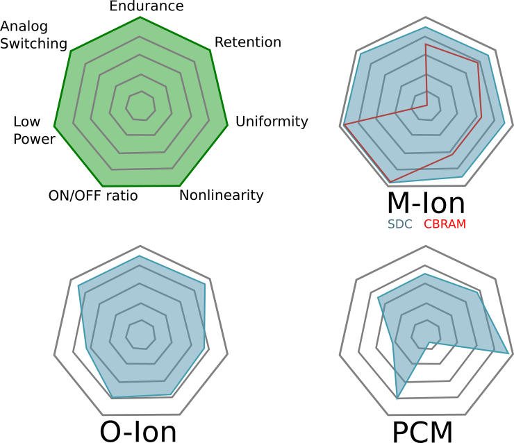
| Section 2.1, ❡1 | “The Metal-ion (M-ion) based devices are generally known as Conductive Bridge RAM (CBRAM) or Electrochemical Metallization Cell (ECM).” | “The Metal-ion (M-ion) based devices are generally known as an Electrochemical Metallization Cell (ECM) and there are two known types: Conductive Bridge RAM (CBRAM) and Self-Directed Channel. |
| Section 2.1, ❡1 | These sequential processes lead to the nucleation and continued growth of the (metallic) filament until the two electrodes become connected, and the device resistance abruptly drops to the LRS. | These sequential processes lead to the nucleation and continued growth of the metallic filament or clusters until the two electrodes become connected, and the device resistance falls. In the case of CBRAM devices this change is abrupt and will drop to the LRS. In the case of SDC devices the drop is a function of the applied voltage-time product, as the device can hold analog state. |
| Section 2.1, ❡1 | Figure 2(b) and (c) show transmission electron microscopy (TEM) images verifying the formation of a complete filament after SET and the rupture of the filament after RESET | Figure 2(b) and (c) show transmission electron microscopy (TEM) images of a CBRAM device verifying the formation of a complete filament after SET and the rupture of the filament after RESET |
| Section 2.1, ❡2 | Originally, chalcogenides were chosen due to the high diffusivity of the active metal species in these films. However, these devices normally suffer from high programming current and very low RESET voltage (comparable to the thermal voltage) that increases accidental reset error, along with material compatibility issues | Originally, chalcogenides were chosen for CBRAM due to the high diffusivity of the active metal species in these films. However, these devices suffered from high programming current and very low RESET voltage (comparable to the thermal voltage) that increased accidental reset error. Researchers later found that the presence of Ge-Ge homopolar bonds in the chalcogenide Ge2Se3 glass facilitated in the incorporation of Ag ions into the Ge2Se3 layer during the first forming step of the device, generating permanent conductive channels that contain Ag agglomeration sites. The amount of Ag within the channel determines the resistance of the device. These devices, termed a Self-Directed Channel (SDC) device overcame the main challenges of CBRAM devices |
| Section 2.1, ❡3 | M-ion based devices have shown several key strengths in- cluding high scalability, fast switching time, low SET and RESET voltage, low current, high ON/OFF, and CMOS compatibility [19, 36–38]. However, device variability and endurance may pose challenges in some applications [38, 39]. The source of the variability is the stochastic nature of the filament creation, where the filament shape and the contact point may not be consistent over switching cycles. | M-ion based devices have shown several key strengths including high scalability, fast switching time, low SET and RESET voltage, low current, high ON/OFF, and CMOS com- patibility [19, 36–38]. Device variability and endurance of CBRAM devices may pose challenges in some applications [38, 39]. The source of the variability in CBRAM devices is the stochastic nature of the filament creation, where the filament shape and the contact point may not be consistent over switching cycles. These challenge are overcome in SDC devices through the creation of the self-organized channel, which constrains and defines the conductive pathways and contact points to the channels. |
| Section 2.1, ❡3 | The endurance issue originates from the fact that the conductive filament is composed of foreign ionic inclusions from the active metal, which may cause stress to the dielectric film and can eventually lead to permanent plastic deformation if programming conditions are not optimally set. As a result, a typical M-ion based device can reach 106 SET/RESET cycles that are sufficient for data storage, … | The endurance issue of CBRAM originates from the fact that the conductive filament is composed of foreign ionic inclusions from the active metal, which may cause stress to the dielectric film and can eventually lead to permanent plastic deformation if programming conditions are not optimally set. As a result, a typical CBRAM device can reach 10^6 SET/RESET cycles. Due to ion migration being confined within channels, a typical SDC device has much higher endurance than CBRAM, 10^9 write-erase cycles or more. |
| Figure 1c |  |
 |
| Figure 11(i,j,k) | 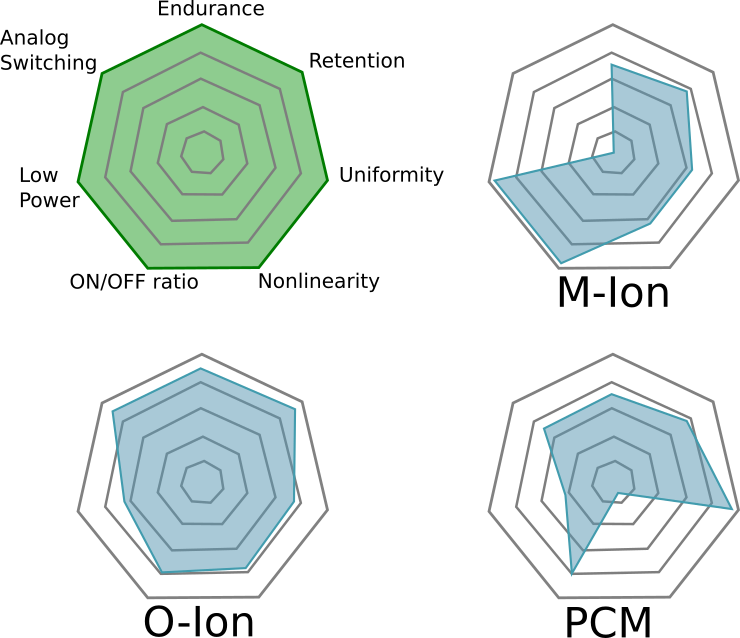 |
 |
Comments on Figure 1
The paper uses three words interchangeably: Metal-Ion, Conductive Bridge RAM (CBRAM) and Electrochemical Metallization Cell (ECM), which is incorrect. They indicate that CBRAM is the only such example of a metal-ion memristor. CBRAM is a sub-type of Metal-Ion memristors, and Knowm SDC devices is another sub-type. There is ample evidence for this categorization. I will quote from section 2 of this open-access paper on Self-directed channel memristors, which was available online November 25, 2016. The review paper was received in March of 2017 and accepted in August of 2017. That’s 341 days for the authors and the journal reviewers to have discovered and included this reference, in case you are wondering. While I would typically let something like this slide for a more focused paper, this is a review article for goodness sake. Doing literature searches is what they were supposed to be doing. Try it yourself–do a Google Scholar search for “CBRAM memristor”. For us the SDC paper is the 3rd result.
…it must be noted that this device should not be confused with another type of ion-conducting device which also uses Ag or Cu ions to change device resistance, referred to as the ‘conductive bridge’ device (often referred to as CBRAM and also as programmable metallization cell, PMC) [10]. Similarities between the SDC and CBRAM devices are that both typically use chalcogenide materials as the active layer such as AsxSy [11], AgInSbTe [12], GexSey, or GexSy [13], [14] and both use an easily oxidizable metal, such as Cu or Ag, to change the device conductivity [2], [10], [11], [12], [13], [14], [15], [16], [17]. However, there are significant differences between the SDC device and CBRAM device. First, the CBRAM device changes resistance through a mechanism involving the formation and dissolution of a conductive filament between the top and bottom electrodes in response to a potential applied across the device [10]. Second, in the CBRAM device a Cu or Ag metal layer in contact with the chalcogenide active layer is the source of metal ions generated by an applied potential across the device. These ions migrate toward the more negative electrode under an applied potential, where they get reduced and build-up a metallic filament towards the positive electrode which eventually bridges the two electrodes and reduces the device resistance [10]. Reversing voltage polarities between the electrodes causes the conductive filament to disperse, thus increasing the device resistance. In the SDC device, the Cu or Ag metal layer cannot be adjacent to the chalcogenide active layer. Third, the largest difference between the SDC and CBRAM type of chalcogenide-based ion-conducting devices is that the CBRAM is typically fabricated using Se-rich or S-rich glasses by either depositing a ternary material (e.g. Ge-S-Ag) to a desired stoichiometry [16], or by photodoping and/or thermally annealing the Ag or Cu metal into the active amorphous material matrix [10], [13], [16], [21], [22], [23]. To achieve the proper concentration of metal in the glass, precise control of the amount of metal included in the chalcogenide and the stoichiometry of the chalcogenide material is required. Both of these are challenging to achieve and are critical to the consistent operation of the CBRAM device [18], [19], [20]. In addition, the photodoping/annealing fabrication methods significantly reduce the maximum temperature exposure of the device during operation and fabrication. Two major factors that contribute to this are: 1) once the Ag or Cu has been added to the material, reduction in the glass transition temperature occurs and with exposure to higher temperatures this can result in crystallization of the glass, which damages device functionality; and 2) the chalcogenides are prone to over saturation by diffusion of the metal layer into the active layer at higher temperatures.
In contrast to CBRAM, the SDC device, Fig. 1, uses a Ge-rich chalcogenide glass, Ge2Se3, and no photodoping or thermal annealing. Also, the SDC device is operational immediately after fabrication. The Ge2Se3 active layer is where device switching occurs; the key feature of this material is the presence of Ge-Ge homopolar bonds. The three layers consisting of Ge2Se3/Ag/Ge2Se3, directly below the top W electrode, mix together during deposition and jointly form the Ag-source layer. This Ag-source layer is not in direct contact with the active layer. This allows the device to have significantly higher processing and operating temperatures (above 250 °C and at least 150 °C, respectively) since Ag does not migrate into the active layer at high temperatures, and the active layer maintains a high glass transition temperature (~350 °C). These processing and operating temperatures are higher than most ion-conducting chalcogenide device types, including the S-based glasses (e.g. GeS) that need to be photodoped or thermally annealed. It is a combination of these factors that allow the SDC device to operate over a wide range of temperatures, including long-term continuous operation at 150 °C. The SnSe layer assists in the selective incorporation of Ag ions into the Ge2Se3 layer. This is done by incorporation of Sn ions during the first forming step of the device, likely near the regions of Ge-Ge bonding within the Ge2Se3 layer [24], [25], [26], [27], [28].
It should be noted that while the layered SDC device structure looks complicated due to the number of material layers, it is actually simpler and more reliable to fabricate than the CBRAM device. The entire deposition of the film layers, including the top electrode, is done in-situ in one processing step using a standard sputter tool. No extra time is required for photodoping or annealing, as is needed for the CBRAM device. Additionally, layer thicknesses are not critical; the active layer could be considered the only thickness sensitive layer, but it has a wide margin of acceptable variation, between 300 and 500 Å. Wafer-to-wafer consistency is therefore high, as across-wafer film thickness variation is not a factor. Because tight controls do not need to be in place for maintaining film thicknesses to tight tolerances, tool qualifications can be done less frequently and a production line could continue for longer periods without being out of specification. Because of this, wafer yields, in terms of number of functional devices per wafer, for the SDC devices are typically >90%.
In contrast, the CBRAM device depends critically on the amount of Ag incorporated into the device during photodoping/annealing. This means that the glass thickness and the Ag thickness need to be well-controlled as slight variations can cause the device to switch poorly (too little Ag) or to become saturated (too much Ag). The photodoping step also depends on good thickness control since the time of light exposure is linked to the amount of Ag incorporated into the device during processing. Consequently, the processes need to be frequently monitored and tools qualified more often. This translates to production down time and frequent poor yields. Additional complications of the CBRAM device fabrication include the device sensitivity to light exposure. As Ag can be photodoped into the device during light exposure, the wafers must be maintained in a dark environment until the risk of photodoping is removed.
In summary, five main factors differentiate the SDC device in terms of operation and fabrication:
1. The device can operate continuously at 150 °C without degradation.
2.No photodoping or thermal annealing is required, saving time, money, and handling risks.
3.The in-situ deposition of all device layers, including the top electrode, occurs with a standard sputter deposition tool in a single step.
4.Film thicknesses in the stack are not critical.
5.Cost is reduced due to a decrease in processing time, use of a single sputter deposition, reduction in qual/down time, and increased yield.
Comments on Figure 11
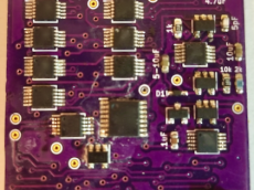
The most striking part about this figure is that the authors believe M-ion devices are incapable of holding analog state, assigning them a solid “zero” on that dimension. Not only can Metal-Ion SDC devices hold an analog state–they can do so at high temperatures. Don’t believe me? Get a Memristor Discovery Kit and check it for yourself. Heck, here I am on December 14th of 2016 demonstrating resistance programming with our inexpensive USB Memristor Discovery USB V0.1 board:
While everybody wants a figure like Figure 11 to help them compare memristor technologies, we need to emphasize that it is a bit misleading and is only relevant if you are doing a relative comparison. This is because some of the properties cannot be co-optimized. For example, as one reduces the energy barriers needed to switch a device the endurance of the device typically goes up because less energy means less wear-and-tear on the device. On the other hand, as energy barriers fall the states become more volatile and data retention is lost–but the energy required to learn goes down.
SDC Fine Points
SDC Memristors are Non-Filamentary
It is important to understand the distinction between the conductive pathway and the channel in a SDC memristor. The channel fills with m-ions at various amounts and does not form a metallic filament. The channel is a permanent feature during normal use, i.e. so long as the device has not been damaged due to a high field and current, the channels structure is constant and acts to confine and guide the flow of m-ions. This is a major distinction between SDC Memristors and filamentary memristors, and it is what puts SDC memristors in a totally seperate class. SDC Memristors should not be classified as filamentary devices.
Layered and Doped
The Knowm SDC memristors are a layered and doped structure, where doping refers to the element introduced into the active channel layer in small amounts. This layered and doped structure facilitates the analog response by modifying the defects in the Ge2Se3 that control Ag+ incorporation. By changing the dopant we can change the properties of the memristor in rather interesting ways. Knowm Carbon-Doped memristors are less incremental, more binary and lower power while Knowm Tungsten-doped memristors are more incremental, analog and higher power.
Closing Thoughts
While I have my irritations with Lu’s group and some of his collaborators, they have done a lot of great work over the years. I remember fondly when I was an advisor to the DARPA SyNAPSE program and I witnessed Wei Lu at HRL’s compound in Malibu. He was there, sweat dripping off of his and his student’s foreheads, a tangle of wires in every direction, showing us his memristors switching. After dreaming about it for so many years–and working with Todd Hylton to conceptualize, formalize and ultimately launch the SyNAPSE program–it was exhilarating to see it happen. I consider myself lucky to have been there and to have witnessed history when HRL paired memristors and CMOS–even if it was not exactly how it was intended to be done. Indeed, not long after this, in the very same room at HRL, I met the late Dr. Hubler and became more acutely aware of the deep connections between thermodynamic self organization and intelligence. While the seeds of Thermodynamic Computing were planted by many people over many years, I feel that this was when those seeds really got a good watering and began to sprout. But that is a story for next time.


Leave a Comment