Introduction
Many memristive materials have recently been reported [1–5], and the trend continues. New designs and materials are being used to create a diverse range of devices and Knowm Inc. is now selling discrete memristors! Memristor models are also being developed and incrementally improved upon [6–10]. Our generalized metastable switch (MSS) memristor model is an accurate model that captures the behavior of memristors at a level of abstraction sufficient to enable efficient circuit simulations while simultaneously describing a wide a range of possible devices [11]. A MSS is an idealized two-state element that switches probabilistically between its two states as a function of applied voltage bias and temperature. A memristor is modeled by a collection of MSSs evolving in time, which captures the memory-enabling hysteresis behavior. In our semi-empirical model, the total current through the device comes from both a memory-dependent (MSS) current component, 

+(1-\phi)I_{\rm s}(V)")
, where ![\phi\in{[0,1]}](https://s0.wp.com/latex.php?latex=%5Cphi%5Cin%7B%5B0%2C1%5D%7D&bg=ffffff&fg=000000&s=0 "\phi\in{[0,1]}")

Why Another Memristor Model?
Frankly, existing memristor models weren’t all that great for the type of devices we are interested in using to build Thermodynamic-RAM, a neuromorphic co-processor based on the principles of AHaH Computing. We also were faced with the problem that most memristors we have seen display some measure of stochastic behavior, and many model assume a deterministic device. We felt that a stochastic model was a more natural fit to actual device properties. An effective memristive device model for our use case should satisfy several requirements. It should accurately model the device behavior, it should be computationally efficient, and it should model as many different devices as possible. Many memristive device models exist, but we felt compelled to create another one which modeled a wider range of devices and, in particular, shows a transition from stochastic binary to incremental analog properties. An AHaH Node, (shown in Figure 1) is not constrained to just one particular memristive device; any memristive device can be used as long as it meets the following criteria: (1) it is incremental and (2) its state change is voltage dependent. Based on our current understanding, the ideal device would have low thresholds of adaptation (<0.2 V), on-state resistance of ∼10 kΩ or greater, high dynamic range, durability, the capability of incremental operation with very short pulse widths and long retention times of a week or more. However, even devices that deviate considerably from these parameters will be useful in more specific applications. For example, short retention times on the order of seconds are perfectly compatible with combinatorial optimizers.
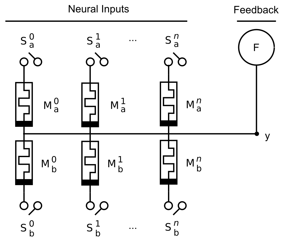
Figure 1. An AHaH Node. An AHaH Node is made up of n Knowm synapses sharing a common output electrode, y. The Knowm synapse and the AHaH Node are analogous to a biological synapse and neuron, respectively. In Thermodynamic-RAM, the number of input synapses can be configured via software and several AHaH Nodes can be connected together to form any desired network topology by a technique called temporal partitioning.
A recent Ag-Chalgogenide memristor from Boise State University device and model hysteresis plot is shown in Figure 2. The model provides common ground from which the diversity of devices can be compared and incorporated into our kT-RAM technology stack.
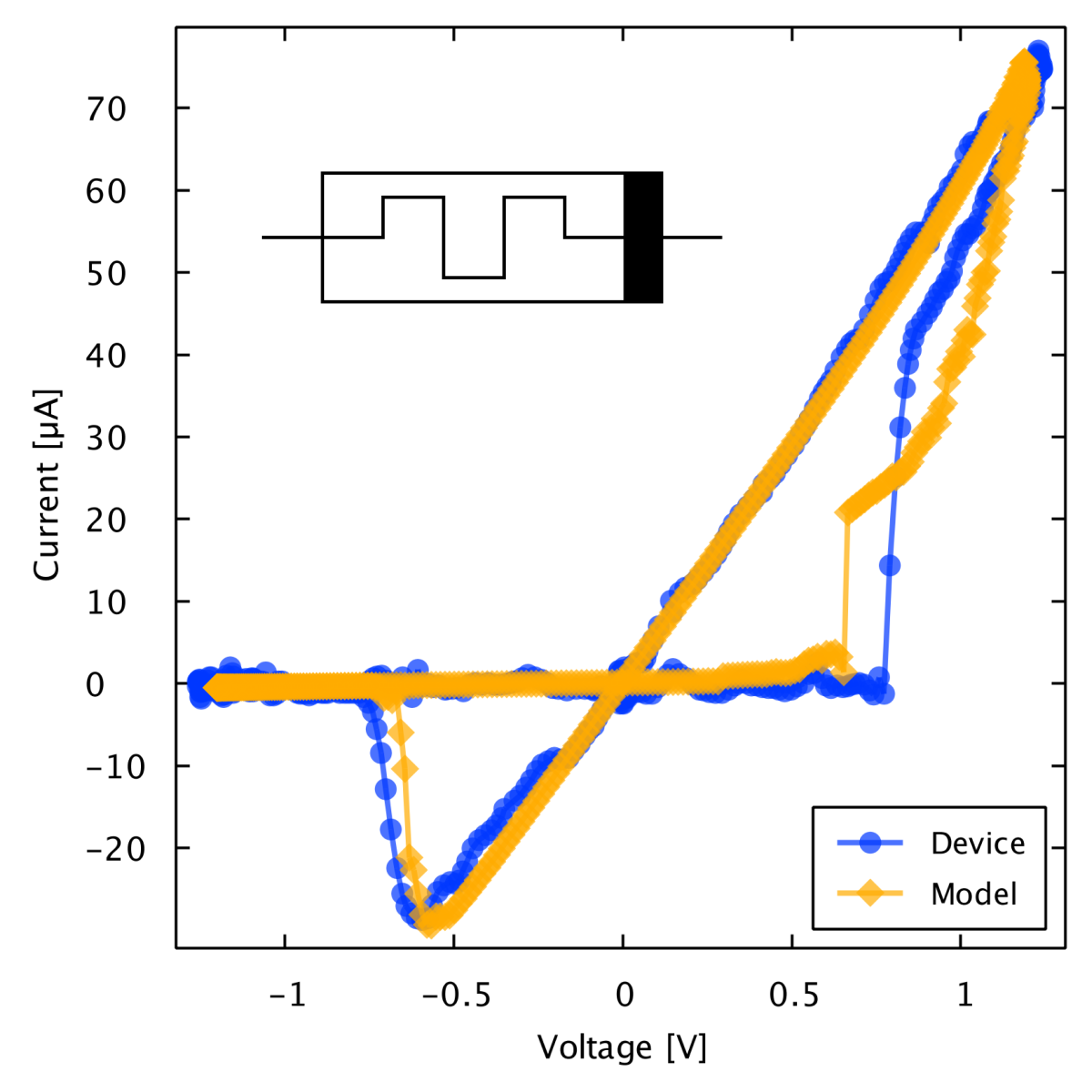
Figure 2. Model and Raw Data Fit for Ag-Chalcogenide Device. Our generalized memristor model captures both the memory and exponential diode characteristics via metastable switch (MSS) and a Skottkey diode and provides an excellent model for a wide range of memritive devices. Here we show a hysteresis plot for a Ag-chalcogenide device from Boise State University along with a fitted model.
Generalized Metastable Switch Memristive Device Model
In our proposed semi-empirical model, the total current through the device comes from both a memory-dependent current component,
, where ")

, where 


}}}} = \alpha \Gamma \left( { V,{V_{\rm A}}} \right)")
and
} \right)")
, where ^{ 1}}")


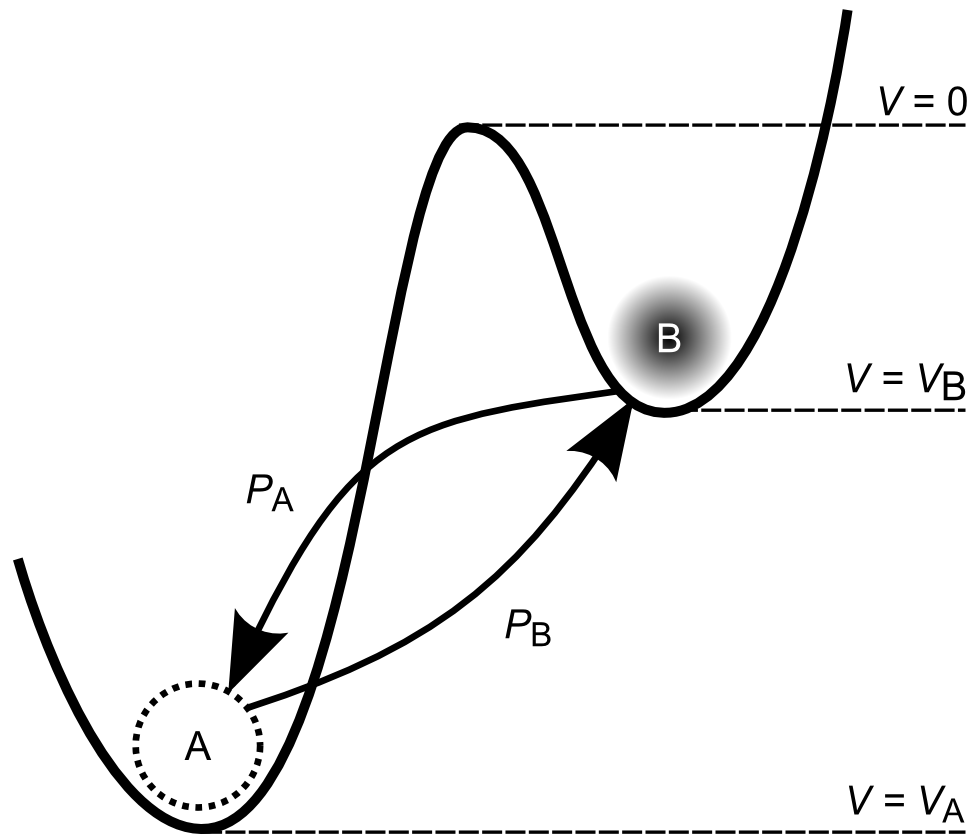
Figure 3. Generalized Metastable Switch (MSS). An MSS is an idealized two-state element that switches probabilistically between its two states as a function of applied voltage bias and temperature. The probability that the MSS will transition from the B state to the A state is given by 
We model a memristor as a collection of
 + N{G_{\rm A}}")
, where 


 = \frac{{n!}}{{k!\left( {n - 1} \right)!}}{p^k}{\left( {1 - p} \right)^{n - k}}")
, where 
 = \frac{{{e^{\frac{{ {{\left( {x - \mu } \right)}^2}}}{{2{\sigma ^2}}}}}}}{{\sqrt {2\pi {\sigma ^2}} }}")
, where 
")

")
} \right) - \mathcal{N}\left( {{N_{\rm B}}{P_{\rm B}},{N_{\rm B}}{P_{\rm B}}\left( {1 -{P_{\rm B}}} \right)} \right)")
. The final update to the conductance of the memristor is then given by:
")
. Reducing the number of MSSs in the model will reduce the averaging effects and cause the memristor to behave in a more stochastic way. As the number of MSSs becomes small, the normal approximation to the binomial distribution breaks down. However, our desired operating regime of many metastable switches, and hence incremental behavior, is within the acceptable bounds of the approximation.
Model Applied to a Variety of Devices
By adjusting the free variables in the generalized memristive device model and comparing the subsequent current-voltage hysteresis loops to four real world memristive device I–V data, matching model parameters were determined as shown in Table 1. The devices include the Ag-chalcogenide [1], AIST [19], GST [20], and WOx [8] devices, and they represent a wide spectrum of incremental memristive devices found in recent publications exhibiting diverse characteristics. Table 1. General memristive device model parameters fit to various devices. The devices used to test our general memristive device model include the Ag-chalcogenide, AIST, GST, and WOx devices. The parameters in this table were determined by comparing the model response to a simulated sinusoidal or triangle-wave voltage to real I–V data of physical devices.
| Device | |
[mS] |
[mS] |
 [V] [V] |
 [V] [V] |
 |
|
|
|
|
|---|---|---|---|---|---|---|---|---|---|---|
| Ag-chalc | 0.32 | 8.7 | 0.91 | 0.17 | 0.22 | 1 | – | – | – | – |
| AIST | 0.15 | 40 | 10 | .23 | .25 | 1 | – | – | – | – |
| GST | 0.42 | .12 | 1.2 | .9 | 0.6 | 0.7 |  |
3.0 | |
3.0 |
 |
0.80 | .025 | 0.004 | 0.8 | 1.0 | .55 |  |
.85 |  |
6.2 |
Figure 4A shows the hysteresis curve of the model and raw Ag-chalcogenide device data driven at 100 Hz with a sinusoidal voltage of 0.25 V amplitude. Additional 1000 Hz and 10 kHz simulations are also shown. The predicted behavior of the model shows a good fit to the physical Ag-chalcogenide device. In fact the model is arguably better than other models (linear ion drift and nonlinear ion drift) tested for a similar device in [21]. Figure 4B shows the predicted response of two series-connected arbitrary memristive devices with differing parameters driven by the sinusoidal voltage as in 5A. The simulation of two devices in series as shown in Figure 4B also displayed expected characteristics and agrees with results in [22] where the linear ion drift model was used. Experiments have not yet been carried out on physical devices to verify this. Figure 4C shows the incremental pulsed resistance change of a single Ag-chalcogenide modeled device for three different pulse train configurations. The three different pulse trains were chosen to show that by changing both the pulse width or the pulse voltage, the modeled behavior is predicted as expected. Figure 4D shows the time response of the Ag-chalcogenide modeled device at frequencies of 100 Hz, 150 Hz, and 200 Hz. Figure 4E shows the simulated response of the Ag-chalcogenide modeled device to a triangle wave of both +0.1 V and -0.1 V amplitude at 100 Hz designed to show the expected incremental prediction of the model. Figure 4F shows additional model fits to the AIST, GST, and WOx devices. As demonstrated, our model can be applied to a wide range of memristive devices from Chalcogenides to metal-oxides and more. The source code for these simulations can be found at https://github.com/timmolter/AHaH with Java class names: AgChalcogenideHysteresisPlotA.java, AgChalcogenideHysteresisPlotB.java, AgChalcogenidePulseTrainPlotC, AgChalcogenideTimePlotD, AgChalcogenideTrianglePlotE, AgInSbTeHysteresisPlot.java, GSTHysteresisPlot.java, and PdWO3WHysteresisPlot.java.
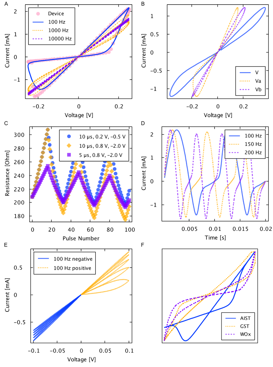
Figure 4. Generalized memristive device model simulations. A) Solid line represents the model simulated at 100 Hz and dots represent the measurements from a physical Ag-chalcogenide device from Boise State University. Physical and predicted device current resulted from driving a sinusoidal voltage of 0.25 V amplitude at 100 Hz across the device. B) Simulation of two series-connected arbitrary devices with differing model parameter values. C) Simulated response to pulse trains of {10 µs, 0.2 V, -0.5 V}, {10 µs, 0.8 V, -2.0 V}, and {5 µs, 0.8 V, -2.0 V} showing the incremental change in resistance in response to small voltage pulses. D) Simulated time response of model from driving a sinusoidal voltage of 0.25 V amplitude at 100 Hz, 150 Hz, and 200 Hz. E) Simulated response to a triangle wave of 0.1 V amplitude at 100 Hz showing the expected incremental behavior of the model. F) Simulated and scaled hysteresis curves for the AIST, GST, and
Symbology
The following symbol is now used internally at Knowm as it is easier to draw by hand and more accurately represents the definition of a memristor. As Leon Chua, the theoretical inventor of the memristor, has said:
“If it’s pinched, it’s a memristor” –Dr. Leon Chua
The bar signifies the device terminal for which when a voltage is applied across the device with the lower-potential on the side of the bar, it will drive the device into a higher conductance state.

Memristor Symbol Knowm
We believe the natural direction for conductance change in a memristor should defined as increasing, as this is how most adaptive dissipative systems in Nature evolve over time. By convention, a bar signifies the lower potential end in other devices like diodes. Furthermore, from an electro-chemistry merged with a semiconductor devices perspective, we believe having the bar on the cathode makes the most since this is where reduction occurs.
Watch online video about this new symbol here: https://vimeo.com/knowm/knowmmemristorsymbolconventions

Memristor Symbol Conventions
Memristor symbol files can be downloaded here:
- Memristor Symbol Knowm 400 px (png)
- Memristor Symbol Knowm 200 px (png)
- Memristor Symbol Knowm 100 px (png)
- Memristor Symbol Knowm 64 px (png)
- Memristor Symbol Knowm (svg)
Conclusion
The generalized metastable switch memristor model presented above does an excellent job at modeling the behavior of a wide range of devices (Ag-chalcogenide, AIST, GST, and
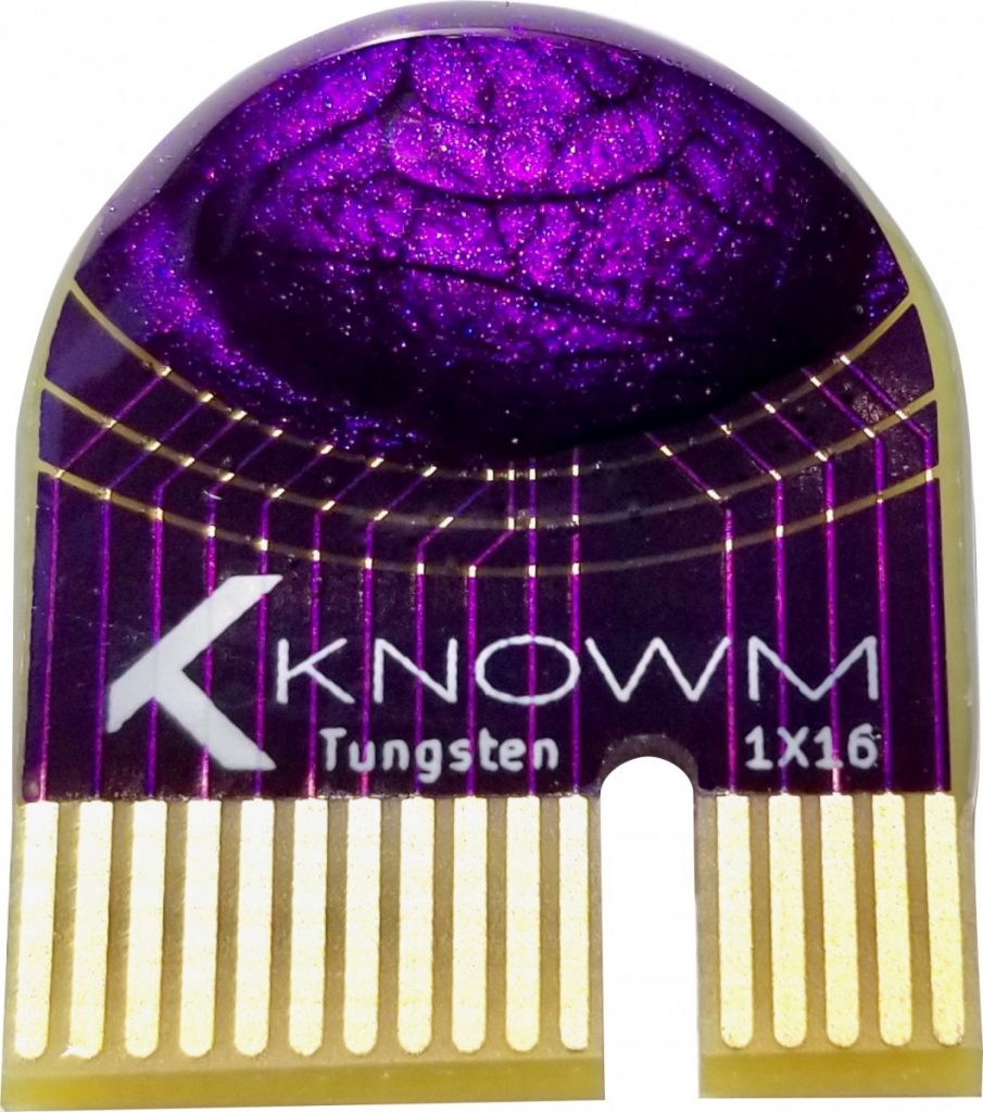
Knowm 1X16 Memristor Array Chip (Front)
The above introduction is a modified excerpt from our 2014 PLoS One paper. To learn more about the theory of AHaH computing and how memristive+CMOS circuits can be turned into self-learning computer architecture using the above AHaH rule, download the paper at: AHaH Computing–From Metastable Switches to Attractors to Machine Learning.
References
- Oblea AS, Timilsina A, Moore D, Campbell KA(2010) Silverchalcogenide based memristor devices. In: Proc. 2010 IEEE International Joint Conference on Neural Networks (IJCNN). pp. 1–3.
- Yang Y, Sheridan P, Lu W (2012) Complementary resistive switching in tantalum oxide-based resistive memory devices. Applied Physics Letters 100: 203112.
- Valov I, Kozicki MN (2013) Cation-based resistance change memory. Journal of Physics D: Applied Physics 46: 074005.
- Hasegawa T, Nayak A, Ohno T, Terabe K, Tsuruoka T, et al. (2011) Memristive operations demonstrated by gap-type atomic switches. Applied Physics A 102: 811–815.
- Jackson BL, Rajendran B, Corrado GS, Breitwisch M, Burr GW, et al. (2013) Nanoscale electronic synapses using phase change devices. ACM Journal on Emerging Technologies in Computing Systems (JETC) 9: 12.
- Choi S, Ambrogio S, Balatti S, Nardi F, Ielmini D (2012) Resistance drift model for conductivebridge (CB) RAM by filament surface relaxation. In: Proc. 2012 IEEE 4th International Memory Workshop (IMW). pp. 1–4.
- Menzel S, Bottger U, Waser R (2012) Simulation of multilevel switching in electrochemical metallization memory cells. Journal of Applied Physics 111: 014501.
- Chang T, Jo SH, Kim KH, Sheridan P, Gaba S, et al. (2011) Synaptic behaviors and modeling of a metal oxide memristive device. Applied Physics A 102: 857–863.
- Sheridan P, Kim KH, Gaba S, Chang T, Chen L, et al. (2011) Device and SPICE modeling of RRAM devices. Nanoscale 3: 3833–3840.
- Biolek D, Biolek Z, Biolkova V (2009) SPICE modeling of memristive, memcapacitative and meminductive systems. In: Proc. 2009 IEEE European Conference on Circuit Theory and Design (ECCTD). pp. 249–252.
- Nugent MA, W MT (2014) Ahah computing-from metastable switches to attractors to machine learning. PLoS ONE 9: e85175.
- Shang DS, Shi L, Sun JR, Shen BG, Zhuge F, et al. (2010) Improvement of reproducible resistance switching in polycrystalline tungsten oxide films by in situ oxygen annealing. Applied Physics Letters 96: 072103.
- Jo SH, Chang T, Ebong I, Bhadviya BB, Mazumder P, et al. (2010) Nanoscale memristor device as synapse in neuromorphic systems. Nano Letters 10: 1297–1301.
- YangJJ,PickettMD,LiX,OhlbergDA,StewartDR,etal.(2008)Memristiveswitchingmechanism for metal/oxide/metal nanodevices. Nature Nanotechnology 3: 429–433.
- Kvatinsky S, Friedman EG, Kolodny A, Weiser UC (2013) TEAM: ThrEshold Adaptive Memristor model. IEEE Transactions on Circuits and Systems I: Regular Papers 60: 211-221.
- Strukov DB, Williams RS (2009) Exponential ionic drift: fast switching and low volatility of thinfilm memristors. Applied Physics A 94: 515–519.
- Pickett MD, Strukov DB, Borghetti JL, Yang JJ, Snider GS, et al. (2009) Switching dynamics in titanium dioxide memristive devices. Journal of Applied Physics 106: 074508.
- Williams RS, Pickett MD, Strachan JP (2013) Physics–based memristor models. In: Proc. 2013 IEEE International Symposium on Circuits and Systems (ISCAS). pp. 217–220.
- Zhang JJ, Sun HJ, Li Y, Wang Q, Xu XH, et al. (2013) AgInSbTe memristor with gradual resistance tuning. Applied Physics Letters 102: 183513.
- Li Y, Zhong Y, Xu L, Zhang J, Xu X, et al. (2013) Ultrafast synaptic events in a chalcogenide memristor. Scientific Reports 3 doi:10.1038/srep01619.
- Pino RE, Bohl JW, McDonald N, Wysocki B, Rozwood P, et al. (2010) Compact method for modeling and simulation of memristor devices: ion conductor chalcogenide-based memristor devices. In: Proc. 2010 IEEE/ACM International Symposium on Nanoscale Architectures (NANOARCH). pp. 1–
- Mladenov VM, Kirilov SM (2012) Analysis of a serial circuit with two memristors and voltage source at sine and impulse regime. In: Proc. 2012 IEEE 13th International Workshop on Cellular Nanoscale Networks and Their Applications (CNNA). pp. 1–6.


Leave a Comment