
In a recent post titled Simulating the Knowm M-MSS Memristor Model Pulse Response with Qucs-S and Xyce, I presented circuit simulations that focus on the dynamic behavior of the M-MSS model’s incremental conductance response to applied square wave pulses. In this post I will continue to explore this behavior by creating basic logic cicuits (i.e. 2-input AND, 2-input OR gates) and perform simulations using discrete memristor elements and sub-circuit models which implement neuromemristive synapses (i.e. AHaH kT-Synapses). I will demonstrate how to configure mixed mode simulations using a 2-output pattern generator contained in the Qucs-S Xyce Digital library to configure square wave pulses with specific pulse timing to produce the truth table inputs to the logic circuits. As part of this tutorial we will also be exploring some additional advanced features of Qucs-S and Xyce for displaying timing diagrams and measuring the power across the memristor elements during the transient simulation. The new Knowm_AHaH library included in the latest release candidate #3 of the Knowm OSS EDA Stack provides AHaH synapse node configurations implemented as sub-circuits to simplify building netlists for simulating the same basic logic circuits designed using discrete memristor components. This new library will be used in future simulations of neuromemristive circuits and machine learning algorithms in hardware.
An example Qucs-S project has been created to perform various experiments that we will later set up on actual memristor devices using the Knowm Memristor Discovery board and associated extender modules. The following experiments are included in the example Qucs-S project AHaH_Logic_prj available in the examples_knowm_oss-eda-0.0.19s-rc3 bundle.
Memristor Experiments Included in the Accompanying Examples
-
ahah_mr_AND2_pl2
(2) Rectangular Pulse sources with positive pulse amplitude of 1V with transient analysis simulating an AHaH 1-2 synapse using discrete memristor elements configured to produce the logic states of a 2-input AND gate.
-
ahah_mr_AND2
Xyce 2-output pattern generator with positive pulse amplitude of 1V with transient analysis simulating an AHaH 1-2 synapse using discrete memristor elements configured to produce the logic states of a 2-input AND gate.
-
ahah_mr_OR2
Xyce 2-output pattern generator with positive pulse amplitude of 1V with transient analysis simulating an AHaH 1-2 synapse using discrete memristor elements configured to produce the logic states of a 2-input OR gate.
-
ahah1-2_synapse_AND2
Xyce 2-output pattern generator with positive pulse amplitude of 1V with transient analysis simulating an AHaH 1-2 synapse using the AHaH 1-2 synapse subcircuit configured to produce the logics state of a 2-input AND gate.
-
ahah1-2i_synapse_OR2
Xyce 2-output pattern generator with positive pulse amplitude of 1V with transient analysis simulating an AHaH 1-2 synapse using the AHaH 1-2i (inverted) synapse subcircuit configured to produce the logic states of a 2-input OR gate.
NOTE: We will be covering the AND2 examples and the AHaH 1-2i Synapse OR2 circuit in this tutorial. The other OR2 circuits are almost identical and can be explored using the same steps as presented here for the corresponding AND2 circuits.
Prerequisites
- Please follow the detailed tutorial Simulating the Knowm M-MSS Memristor Model Using Qucs-S with Xyce to learn the basics of creating a Qucs-S schematic file for use with Xyce to perform a transient simulation of the M-MSS model using an AC sinusoidal waveform.
-
Please follow the installation and configuration of your OSS EDA Environment Simulating the Knowm M-MSS Memristor Model Pulse Response with Qucs-S and Xyce.
NOTE: The instructions there should be almost identical to the ones necessary for installing release candidate #3 used for this tutorial.
- Update to the latest release candidate #3 of the
Knowm OSS EDA Stack. It is available formacOS 10.12 SierraandUbuntu 16.04 LTS (Xenial Xerus). This post covers installation and use on macOS and support for Xyce (Serial) simulations only. The included versions of Qucs-S (0.0.19S) and Xyce 6.6 include libraries for amd64 architectures. Support for other architectures and operating systems are under development and will be released when available.
Download and install the latest release candidate #3 from these links.
MacOS Sierra 10.12 QUCs
MacOS Sierra 10.12 Knowm Examples
MacOS Sierra 10.12 Xyce
Linux QUCs
Linux Knowm Examples
Linux Xyce
Overview
The following discussion of simulation of memristor logic circuits was developed based on the results of a paper presented by Frey, et. al. titled: “Investigating Power Characteristics of Memristor-based Logic Gates and Their Applications in a Security Primitive”. You may want to review this paper before or concurrently while working through this tutorial. The following configurations are the inspiration for the circuits we have configured here.
Memristor Logic Circuits
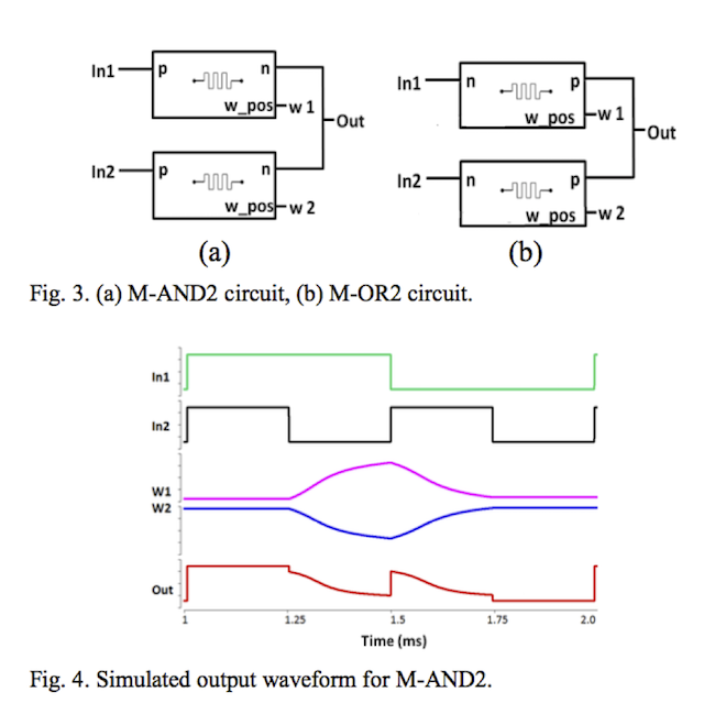
- We will also be using AHaH nodes which will be introduced in a following section. The basic configuration of the AND and OR gate presented use the AHaH 1-2 configuration.
AHaH Logic Gates Based on Memristor Pairs
Open the AHaH Discrete Memristor AND2 Schematic diagram
-
Double click the
AHaH_Logic_prjto automatically open theContenttab. -
Select the
ahah_mr_AND2_2pl.schfrom theSchematicslist in the Contents tab of the Main Dock.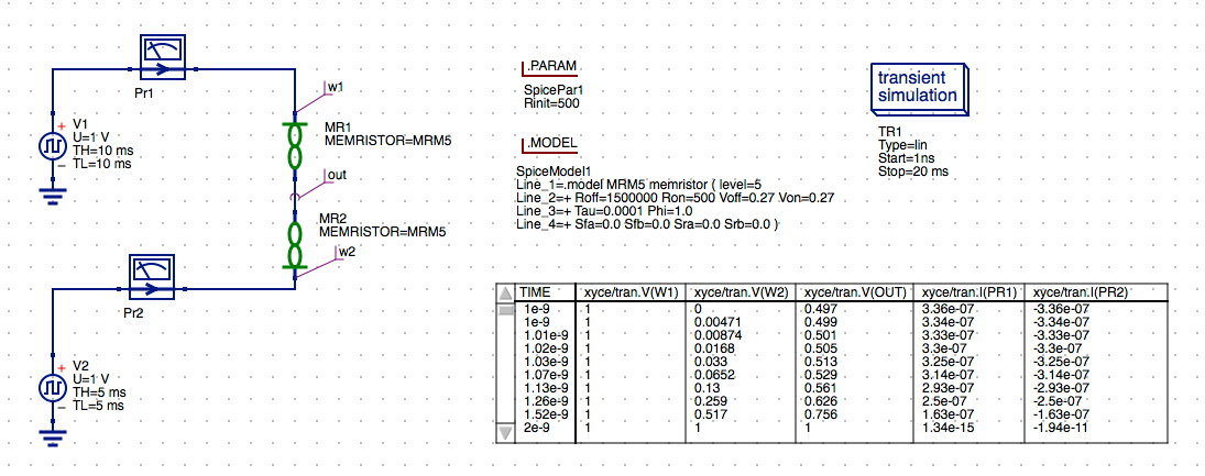
AHaH Memristor AND2 with Rectangle Pulses
NOTE: We are using the AHaH 1-2 synapse
ANDconfiguration from the diagram above and the .Model directiveMRM5, and the M-MSS model from theKnowm_Memristor_Technologylibrary has been assigned for both theMR1andMR2memristor symbols. We have increased the ratio for the Ron and Roff parameter values in the models as discussed in the Frey paper in order to the minimum and maximum values as measured at the output voltage across the divider network.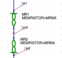
AHaH Memristor 1-2 Configuration
Pulse Voltage Source properties
-
Double click
V1symbol on the schematic to open the parameters and review the settings for theRectangle pulsesource.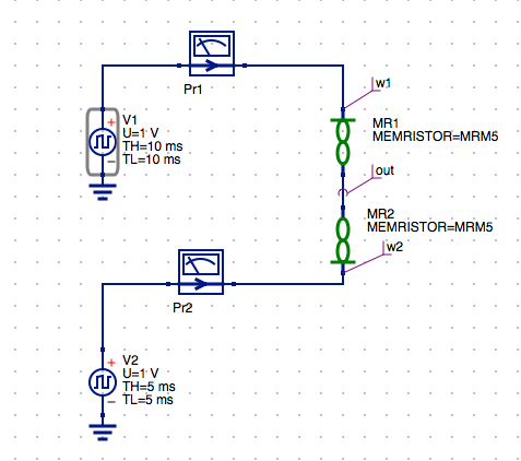
Select V1 Pulse Source
-
Select the
Urow in the properties table. -
The voltage is set to
1 Vso the output will be from 0V to 1V. -
Select the
THrow in the properties table determine the time duration of the high pulses. -
We’ve set this value to
10 msto specify a 10 mspulse width. -
Similarly the
TLrow in the properties table determine the time duration of the low pulses. I have set this also to10 msto specify a 20msperiod.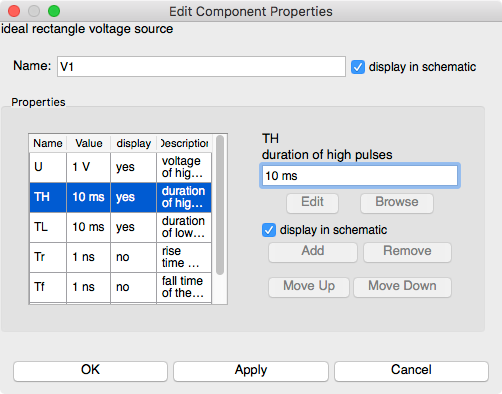
V1 Pulse Source Settings
-
Click
Applyto set the frequency value. -
Click
OKto exit the properties dialog. -
Similarly you can double click
V2symbol on the schematic to open the parameters and review the settings for second theRectangle pulsesource.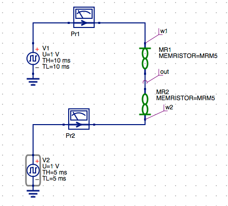
Select V2 Pulse Source
NOTE: The parameters for V2 are set to be half of the period of V1. This will give us twice the number of pulses on the input of the memristor MR2 and allow use to generate the truth table for the gate inputs.
Other Schematic Components
- We have configured two
current probesnamedPr1andPr2that are used to measure the current flowing through each memristor as the pulses are applied to the circuit. -
There are also the
Namenodesw1andw2which will provide the voltage measured across the two memristors MR1 and MR2 respectively and represent the change of the weights and the memristor states based on the change in the conductance in each branch of the synapse. -
The
outnamed node provides the positive voltage for the voltage divider at the junction of theMR1amdMR2memristors which defines the logic state of the synapse which should should0 Vor1 Vat the maximum pulse values.
Transient Simulation Settings
-
Double click on the
transient simulationsymbol to open the setup parameters dialog. -
I have entered
20 msin thestopfield to coincide with the settings for the rectangle pulse sources total period. -
Entering
101in the number value field to set a 200 us step size.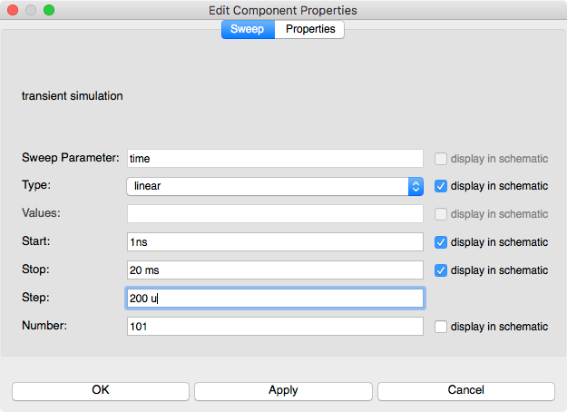
Transient Simulation Settings
-
Click
Applyto save the changes. -
Click
OKto exit the properties dialog.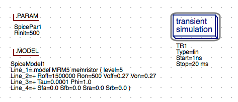
Transient Simulation Parameters
Save the Schematic Diagram File
-
The filename
ahah_mr_AND2_2pl.schhas been used for this example schematic. -
Click the
Savebutton on the toolbar to save the schematic file.

Save Toolbar Button
Run a Simulation
- Press
F2or selectSimulatebutton on the toolbar.

Run Simulation Toolbar Button
-
Check simulation for
errorsorwarnings. See the status bar at the bottom of the Qucs windowlower right corner. -
Click the
Exitbutton to close theSimulationwindow.
View the Tabular Results
-
Check the
Tabularresults.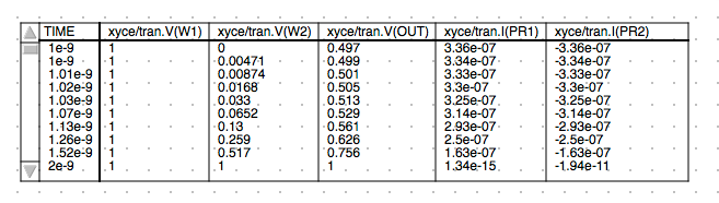
Tabular Results
Cartesian Plot of Memristor-based AND2 Gate ( V vs. Time ) Results
-
You should also observe the results in the specified Cartesian plot defined in the schematic.
Voltage Inputs, Ouput vs. Time
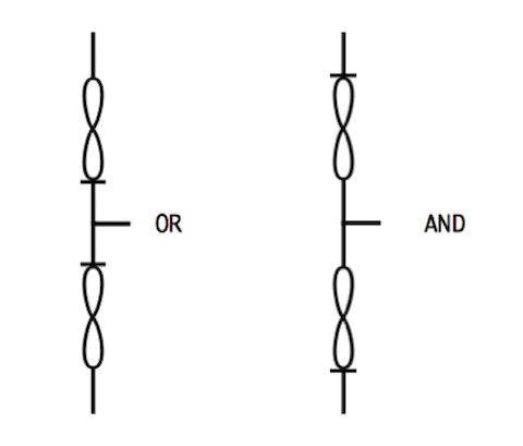
NOTE: The results contain multiple pulses of the
1Vamplitudes forw1andw2we defined in theRectangle Pulsesettings. This provides the 4 states of the AND gate for the following truth table.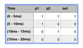
AND2 Circuit Truth Table
-
In the first 5 ms both p1 and p2 are positive
1 Vso theoutstate is also positive1 Vor logic 1.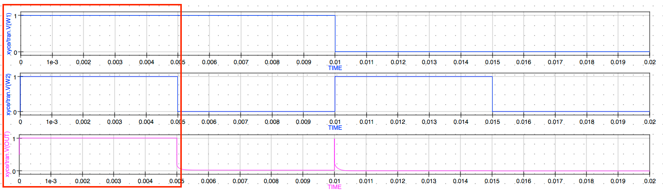
First Logic State ( 0 – 5ms )
-
In the next 5 ms both p1 is positive
1 Vbut p2 is0Vso theoutstate is0 Vor logic 0.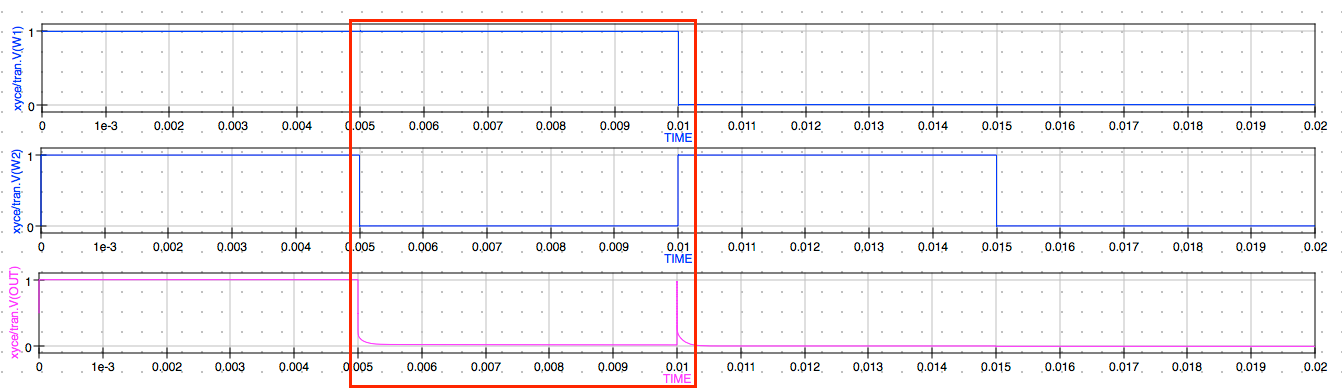
Second Logic State ( 5ms – 10ms )
-
In the next 5 ms both p1 is
0 Vbut p2 is1 Vso theoutstate is still0 Vor logic 0.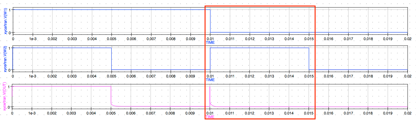
Third Logic State (10ms – 15ms)
-
In the last 5 ms both p1 and p2 are positive
0 Vso theoutstate is also positive0 Vor logic 0.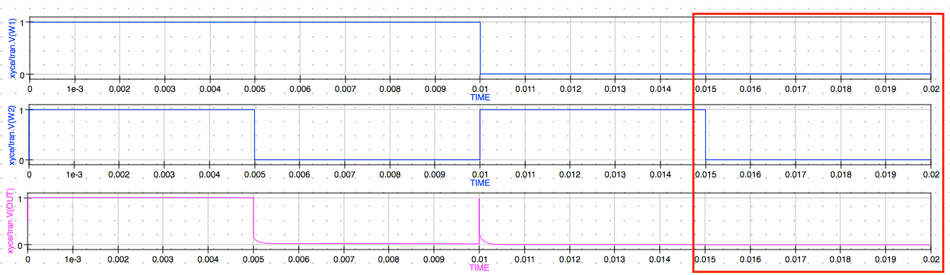
Fourth Logic State (15ms – 20ms)
Open the Schematic diagram
-
Double click the
AHaH_Logic_prjto automatically open theContenttab. -
Select the
ahah_mr_AND2.schfrom theSchematicslist in the Contents tab of the Main Dock.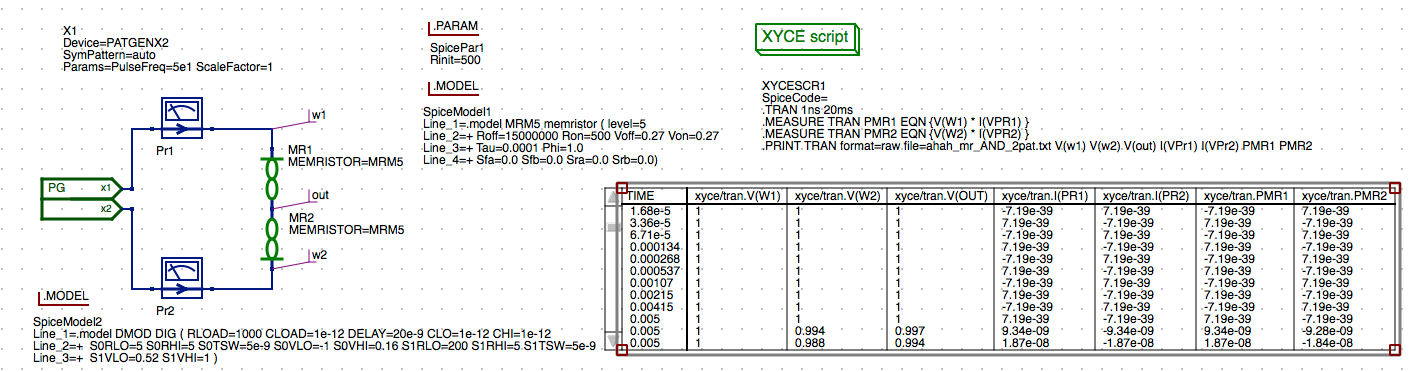
AHaH 1-2 AND2 Schematic
NOTE: Again we are using is the AHaH 1-2 synapse
ANDconfiguration from the diagram above and the .Model directiveMRM5, the M-MSS model from theKnowm_Memristor_Technologylibrary has been assigned for both theMR1andMR2memristor symbols.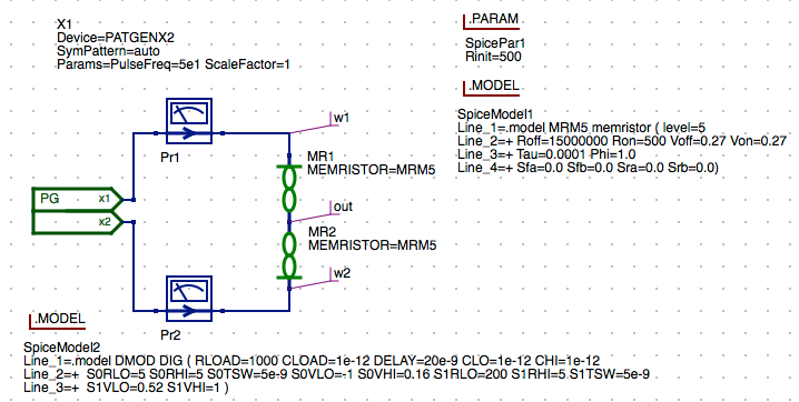
AHaH 1-2 Logic AND Configuration
Configure the 2-Pattern Pulse Gererator Voltage Source
-
The
PATGENX2was added to replace the 2 rectangle pulse sources in the schematic. This is a component found in theXyce Digitallibrary components list.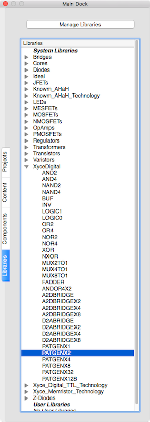
Xyce 2-ouput Pattern Gen
-
Double click
PGsymbol on the schematic to open the parameters and review the settings for thePATGENX2pulse generator source.NOTE: The definition of the component specifies the
x2source output to be 0.5 the period ofx1.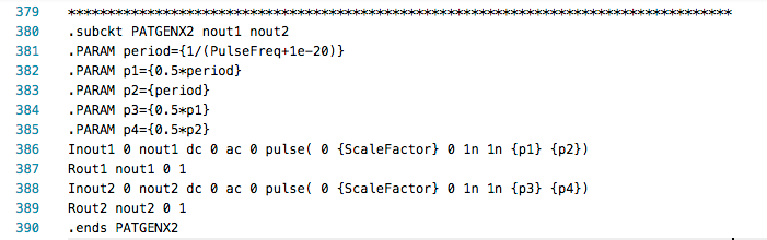
Sub-circuit Definition for Xyce Digital PATGENX2
-
The frequency of the pulse generator is set using
PulseFreq = 5e1. Setting the frequency to5e1will give us a 20 ms period on thex1source output.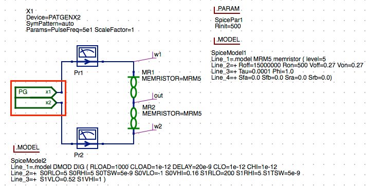
Select PATGENX2 Component
-
We have set the parameter
ScaleFactor = 1will set the voltage on x1 and x2 outputs to1 Vso both will transition from 0 V to 1 V for their low and high output states.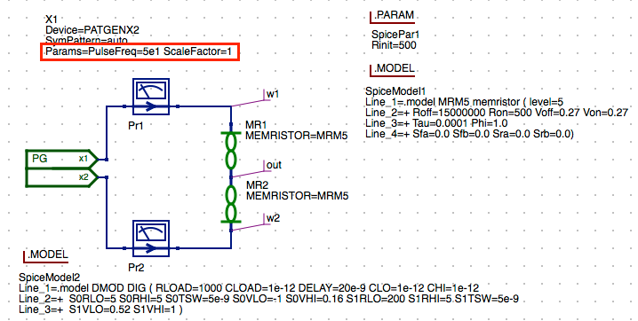
PATGENX2 Pulse Parameters
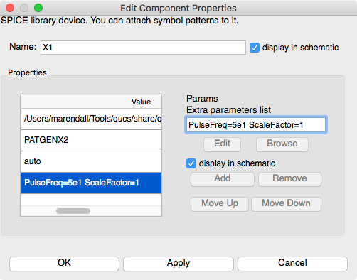
Xyce PATGENX2 Settings
-
Click
Applyto set the frequency value. -
Click
OKto exit the properties dialog. -
The updated parameters for the X1 Sub-circuit are displayed for the PATGENX2 component.

Xyce PATGENX2 Setup
NOTE: Again the parameters for x2 are set to be half of the period of x1. This will give us twice the number of pulses on the input of the memristor MR2 and allow use to generate the truth table for the gate inputs.
- Select .Model directive
DMOD, from theXyce Digital Technologylibrary model from theKnowm_Memristor_TTL_Technologylibrary to assign for it to thePATGEN2Xpulse generator symbol.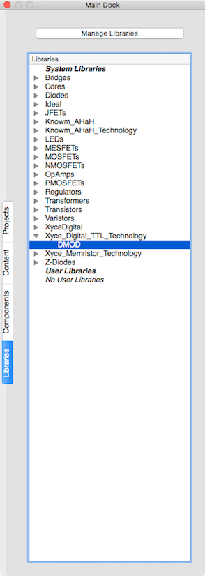
Xyce Digital TTL Tech – DMOD Model
NOTE: The .Model directive for all
Xyce Digitalcomponents use the modelDMODwhich is of typeDIGas defined in the digital library model source.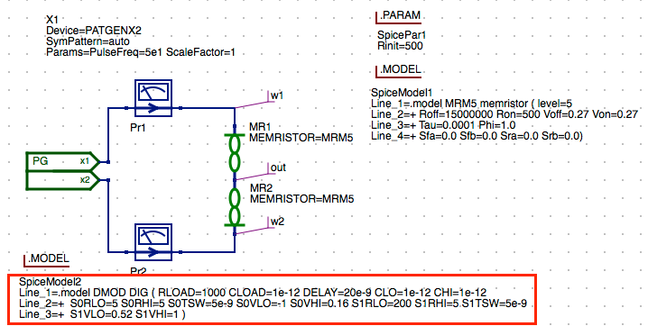
Xyce PATGENX2 Model Parameters
Configure the Transient Simulation in the XYCE Script
-
The
XYCE scriptcomponent symbol has been added to the schematic to define the transient analysis and variables to be output by the Xyce .PRINT statement.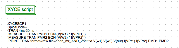
Xyce Script
-
The
.TRANstart and end time have been set to1nand20 msrepectively.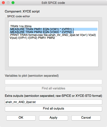
Xyce Script Settings
-
Notice that we have also introduced a new powerful feature of the Xyce script
.MEASURE. This provides a means of calculating a analytical quantity during each time step of the transient simulation. Here we have defined the equationEQN {V(W1)*I(VPR1)}andEQN {V(W2)*I(VPR2)}which will compute the powerPMR1andPMR2through each memristor during the simulation and put result in an output array that can be plotted or used in post-analysis routines. -
Click
Applyto save the changes. -
Click
OKto exit the properties dialog.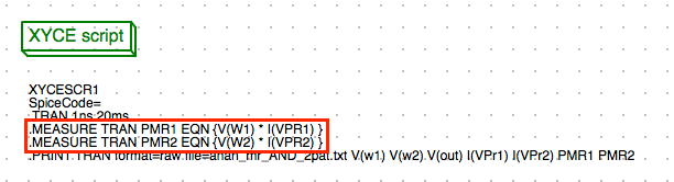
Xyce .MEASURE Directive
Save the Schematic Diagram File
- Click the
Savebutton on the toolbar to save changes to theahah_mr_AND2.schschematic file.
Save Toolbar Button
Run a Simulation
-
Press
F2or selectSimulatebutton on the toolbar.
Run Simulation Toolbar Button
-
Check simulation for
errorsorwarnings. See the status bar at the bottom of the Qucs windowlower right corner. -
Click the
Exitbutton to close theSimulationwindow.
View the Tabular Results
-
Check the
Tabularresults.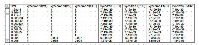
Tabular Results
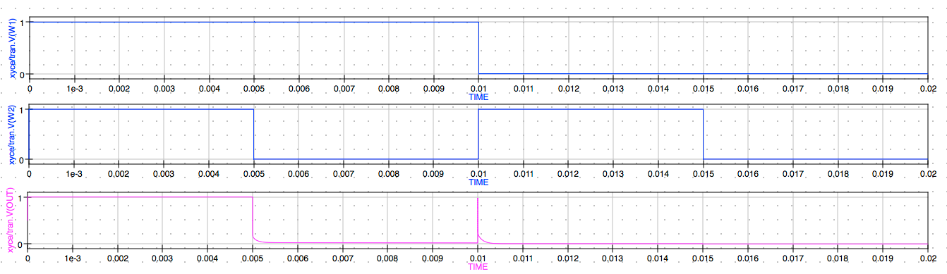
Timing Diagram of Memristor-based AND2 Gate ( V vs. Time ) Results
-
You can display the timing results in the specified
Timing Diagramplaced from thediagramsin the Components tab of the Main Dock.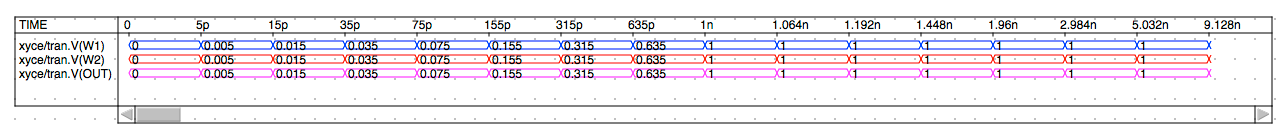
Timing Diagram
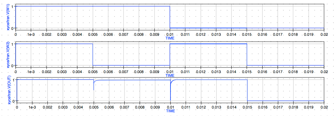
Cartesian Plot of Memristor-based AND2 Gate ( V vs. Time ) Results
-
You should also observe the results in the specified Cartesian plot defined in the schematic.
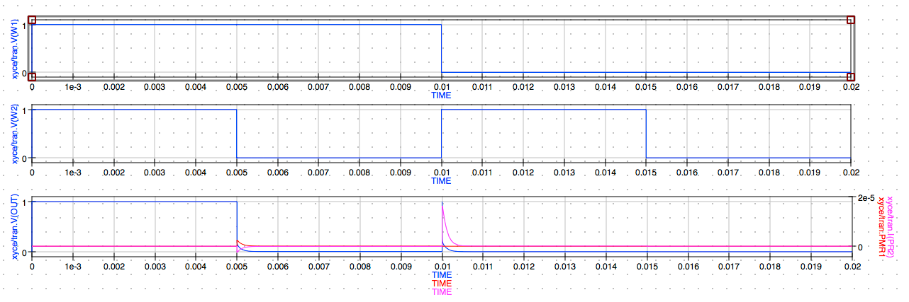
Voltage Input, Output with Memristor Power vs. Time
NOTE: The results contain multiple pulses of the
1Vamplitudes forw1andw2we defined in thePATGENX2settings. This plot not only provides the 4 states of the AND gate as shown before but we have also plotted the calculated powerPMR1andPRM2vsV(OUT)and provided those quantites on the Y2 axis of the plot.
Open the AHaH 1-2 Synapse AND2 Schematic diagram
-
Double click the
AHaH_Logic_prjto automatically open theContenttab. -
Select the
ahah1-2_synapse_AND2.schfromSchematicsin the Contents tab of the Main Dock.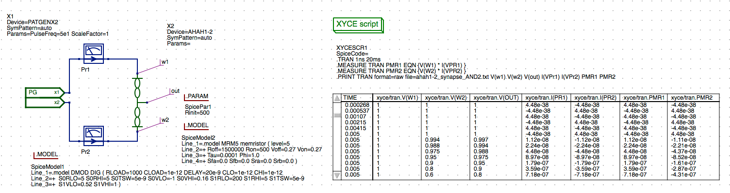
AHaH 1-2 Synapse AND2 Circuit
-
We have selected the
AHaH1-2symbol from theKnowm_AHaHlibrary and placed it on the schematic.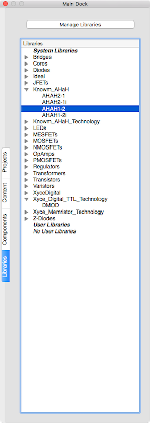
Select AHaH1-2 from Knowm_AHaH Lib
-
The sub-circuit
X2defines the sub-circuit provided for theAHaH1-2 synapseand replaces the two discrete memristors MR1 and MR2 from the last exercise.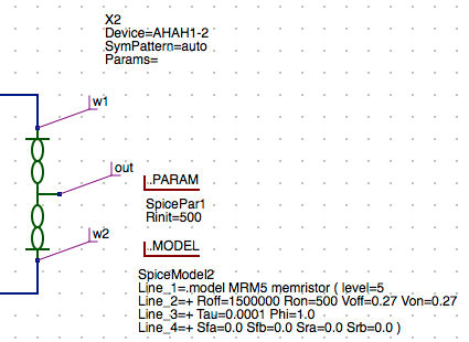
AHaH 2-1 Synapse
NOTE: Again we are using is the AHaH 1-2 synapse
ANDconfiguration from the diagram above and the .Model directiveMRM5, the M-MSS model from theKnowm_Memristor_Technologylibrary has been assigned for both theX2sub-circuit memristor symbols. -
The parameters for the AHaH1-2 component are already set so no further setup is necessary other than specifying the
Rinitparameter using the.PARAMcomponent from the SPICE specfic sections drop-down list in the Components tab of the Main Dock.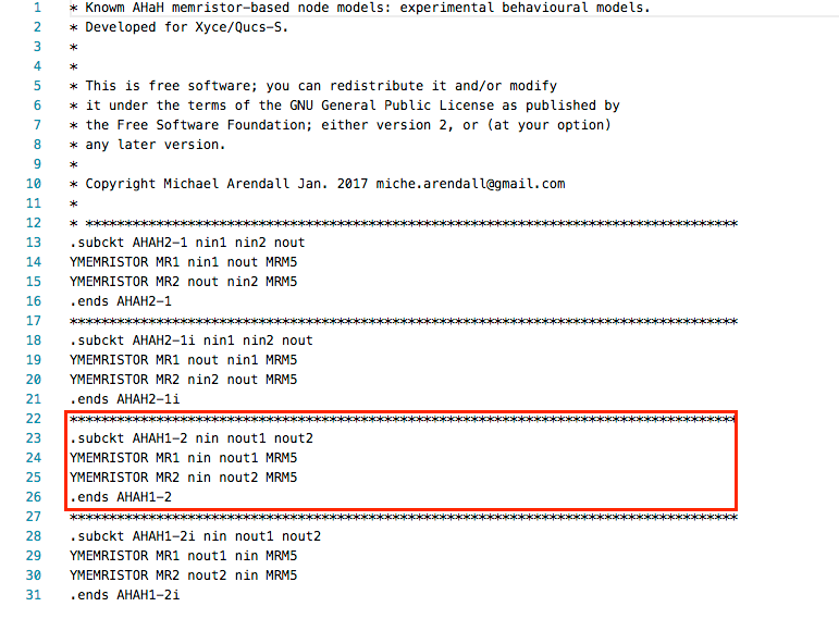
Knowm_AHaH Lib
Save the Schematic Diagram File
- Click the
Savebutton on the toolbar to save changes to theahah1-2_synapse_AND2.schschematic file.
Save Toolbar Button
Run a Simulation
- Press
F2or selectSimulatebutton on the toolbar.
Run Simulation Toolbar Button
-
Check simulation for
errorsorwarnings. See the status bar at the bottom of the Qucs windowlower right corner. -
Click the
Exitbutton to close theSimulationwindow.
View the Tabular Results
-
Check the
Tabularresults.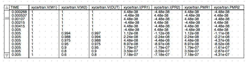
Tabular Results
Cartesian Plot of Memristor-based AND2 Gate ( V vs. Time ) Results
-
You should also observe the results in the specified Cartesian plot defined in the schematic.
Voltage Inputs with Power, Output vs. Time
NOTE: Again the results are the same as shown before using the discrete memristors and contain multiple pulses of the
1Vamplitudes forw1andw2we defined in thePATGENX2settings. This plot not only provides the 4 states of the AND gate as shown before but we have also plotted the calculated powerPMR1,PRM2vsV(W1),V(W2)respectively.
Open the AHaH 1-2i Synapse OR2 Schematic diagram
-
Double click the
AHaH_Logic_prjto automatically open theContenttab. -
Select the
ahah_1-2i_synapse_OR2.schfrom theSchematicslist in the Contents tab of the Main Dock.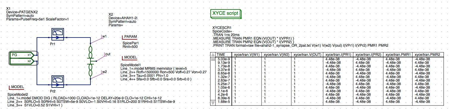
AHaH 1-2i Logic OR2 Circuit
-
For this example we are using is the AHaH 1-2i (inverted) synapse
ORconfiguration from the diagram above and the .Model directiveMRM5, the M-MSS model from theKnowm_Memristor_Technologylibrary has been assigned for both theMR1andMR2memristor symbols.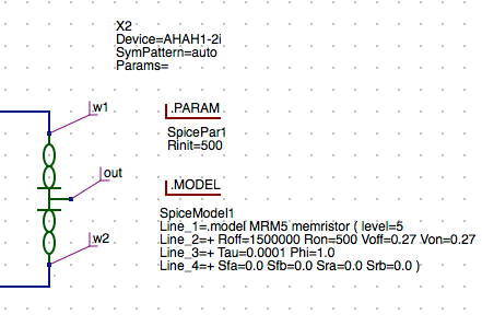
AHaH 1-2i Synapse
Observe the 2-Pattern Pulse Gererator Voltage Source
-
The
PATGENX2was introduced in the previous AND2 schematic to replace the 2 rectangle pulse sources in the schematic. Again, for the OR2 schematic this is a component found in theXyce Digitallibrary components list.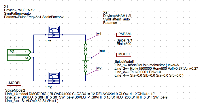
Xyce PATGENX2 Model and AHaH 1-2i Synapse
-
Again the
PGsymbol on the schematic is associated with sub-circuit X1 and the parameters have been set for thePATGENX2pulse generator source. -
The frequency of the pulse generator is set using
PulseFreq = 5e1. Setting the frequency to5e1will give us a 20 ms period on thex1source output. -
We have set the parameter
ScaleFactor = 1will set the voltage on x1 and x2 outputs to1 Vso both will transition from 0 V to 1 V for their low and high output states.NOTE: The definition of the component specifies the
x2source output to be 0.5 the period ofx1.
Again the parameters forx2are set to be half of the period ofx1. This will give us twice the
number of pulses on the input of the memristorMR2and allow use to generate the truth table for
the gate inputs. -
The .Model directive
DMOD, has been selected from theXyce Digital Technologylibrary model to assign for it to thePATGEN2Xpulse generator symbol.NOTE: The .Model directive for all
Xyce Digitalcomponents use the modelDMODwhich is of typeDIGas defined in the digital library model source.
Transient Simulation Configuration in the XYCE Script
-
The
XYCE scriptcomponent symbol has been added to the schematic to define the transient analysis and variables to be output by the Xyce .PRINT statement.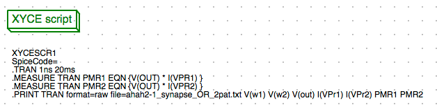
Xyce Script for Transient Simulation
-
The
.TRANstart and end time have been set to1nand20 msrepectively. -
Notice that we have again included the
.MEASURElines. This provides a means of calculating a analytical quantity during each time step of the transient simulation. Here we have defined the equationEQN {V(W1)*I(VPR1)}andEQN {V(W2)*I(VPR2)}which will compute the powerPMR1andPMR2through each memristor during the simulation and put result in an output array that can be plotted or used in post-analysis routines.
Save the Schematic Diagram File
- Click the
Savebutton on the toolbar to save changes to theahah_1-2i_synapse_OR2.schschematic file.
Save Toolbar Button
Run a Simulation
- Press
F2or selectSimulatebutton on the toolbar.
Run Simulation Toolbar Button
-
Check simulation for
errorsorwarnings. See the status bar at the bottom of the Qucs windowlower right corner. -
Click the
Exitbutton to close theSimulationwindow.
View the Tabular Results
-
Check the
Tabularresults.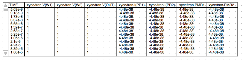
Tabular Results
AHaH 1-2i OR2 Gate Cartesian Plot ( V vs. Time ) Results
-
Observe the results in the specified Cartesian plot defined in the schematic.
Voltage Inputs, Output vs. Time
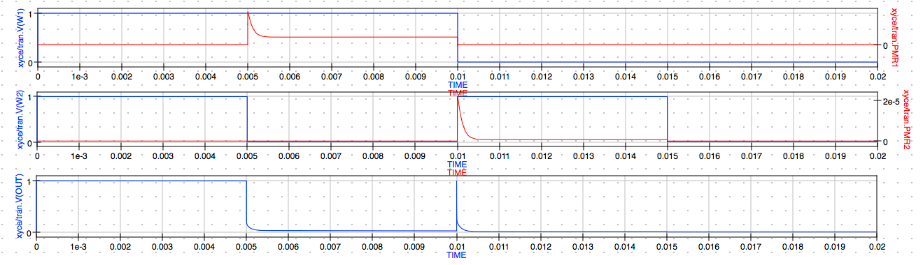
NOTE: The results contain multiple pulses of the
1Vamplitudes forw1andw2we defined in thePATGENX2settings. This plot not only provides the 4 states of the AND gate as shown before but we have also plotted the calculated powerPMR1andPRM2vsV(OUT)and provided those quantites on the Y2 axis of the plot.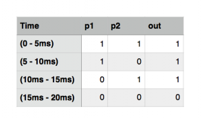
OR Gate Truth Table
-
In the first 5 ms both p1 and p2 are positive
1 Vso theoutstate is also positive1 Vor logic 1.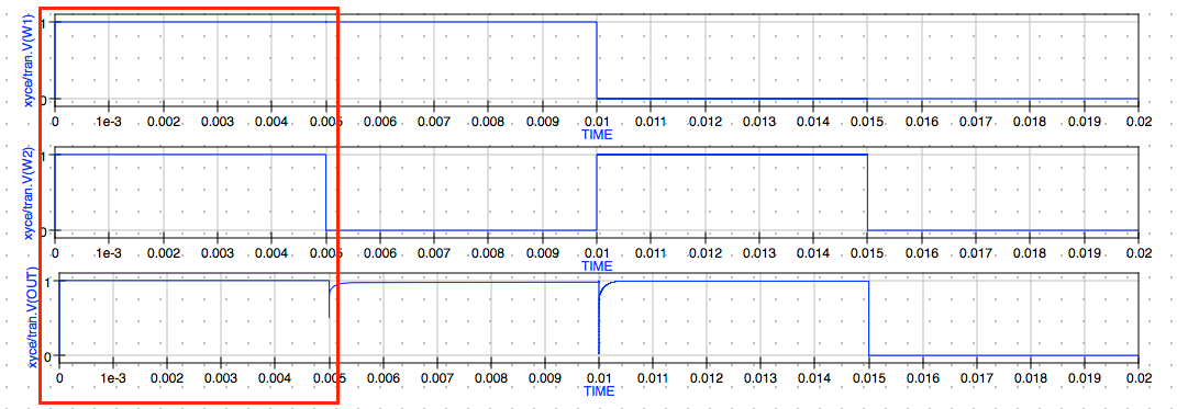
First Logic State ( 0 – 5ms )
-
In the next 5 ms both p1 is positive
1 Vbut p2 is0Vso theoutstate is1 Vor logic 1.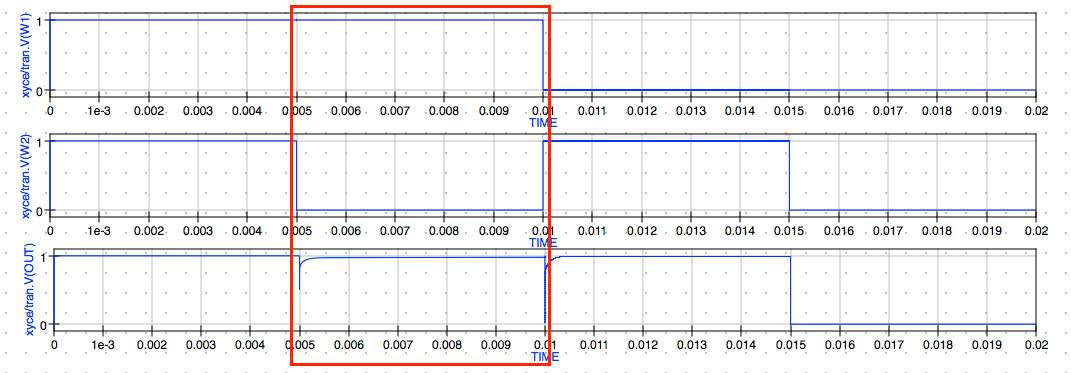
Second Logic State ( 5ms – 10ms )
-
In the next 5 ms both p1 is
0 Vbut p2 is1 Vso theoutstate is still1 Vor logic 1.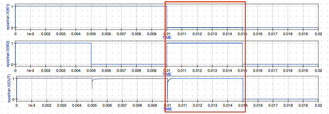
Third Logic State ( 10ms – 15ms )
-
In the last 5 ms both p1 and p2 are positive
0 Vso theoutstate is also positive0 Vor logic 0.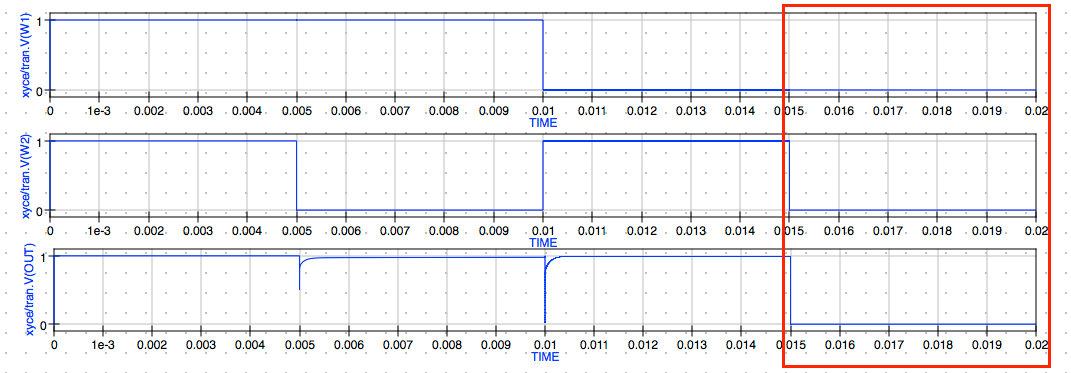
Fourth Logic State ( 15ms – 20ms )
That completes this tutorial. Try some of the other example schematic files available in the AHaH_Logic_prj project. All of these experiments use common features presented here. In our next tutorial we will explore more circuits using AHaH nodes that we’ve presented here to simulate machine learning methods.
You should also checkout the documentation and other examples listed in the Qucs 0.0.19 and Qucs-S 0.0.19 documentation available on the web at the following URLs.
- Qucs 0.0.19 Help: https://qucs-help.readthedocs.io/en/0.0.19/subcircuit.html
- Qucs-S 0.0.19 Help: https://qucs-help.readthedocs.io/en/spice4qucs/SPICEComp.html
- Qucs-S Bugtracker: https://github.com/ra3xdh/qucs/issues
- Qucs-S Sub-project Home Webpage: https://ra3xdh.github.io/
Other References
- What is Qucs?
- What can all be installed from Sourceforge?
- Qucs Website: http://qucs.sourceforge.net/
- Main Repository: https://sourceforge,net/p/qucs/git/ci/master/tree/
- Mirror Repository: https://github.com/Qucs/qucs
- Mailing lists: http://sourceforge.net/p/qucs/mailman/
- Forum: http://sourceforge.net/p/qucs/discussion/
- Bug trackers:
- Source code documentation:
- Wiki: https://github.com/Qucs/qucs/wiki
Further Resources
- Knowm Memristors
- The Generalized Metastable Switch Memristor Model
- Simulating the Knowm M-MSS Memristor Model Using Qucs-S with Xyce
- The Problem is Not HP’s Memristor–It’s How They Want To Use It
- The Joglekar Resistance Switch Memristor Model in LTSpice
- Build Xyce from Source for ADMS Verilog-A Model Integration
- The Pershin Voltage Threshold Memristor Model in NGSpice
- memristor-models-4-all Project on Github


Leave a Comment