History and Evolution of the Device
The first patented chalcogenide ion-conducting memristor was Conductive-Bridging RAM (CBRAM), developed at Arizona State University (ASU) by Kozicki. It was patented in 1998 [1,2] and assigned to Axon Technologies, who in turn licensed the technology to Micron Technology and others [3]. The technology proved difficult to manufacture, and was further modified and improved over the years by several companies, including Micron [4,5].
The chalcogenide ion-conducting memristor went in a different technological direction with the invention of the SDC device [6-7]. This device uses a metal-chalcogenide layer between a specific type of chalcogenide with homopolar bonds on the non-chalcogen atoms (Ge2Se3 or similar), which removes the need to photodope the chalcogen with a mobile metal, such as Ag. The SDC device is not critically dependent on the amount of Ag doped into the glass layer since it does not require any photodoping [8], resulting in an easier to manufacture and more reliable device with thermal stability.
Self Directed Channel Memristor
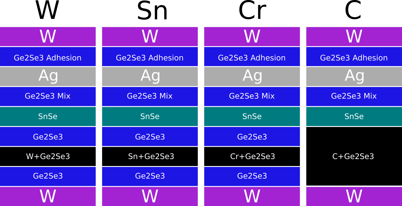
Innovating further on the SDC device, Campbell developed at Boise State University (BSU) a way to alter the device electrical properties by metal doping of a chalcogenide layer, and sandwiching that layer between two undoped layers. The type of metal that is doped in the chalcogenide layer determines the device electrical properties, including threshold switching voltages, resistance states achievable, resistance state retention, capacitance and charge storage, as well as the resistance change mechanism (i.e. phase change or ion conduction). Tunable device electrical parameters are critical to the development of analog applications of memristors such as neuromorphics. This innovation was patented in 2015, assigned to Boise State University, and licensed to Knowm Inc. [9,10].
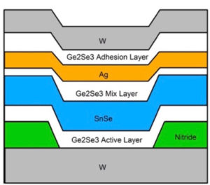
Knowm Memristor Material Stack
References
- Kozicki and West, US Patent 5,761,115 “Programmable metallization cell structure and method of making same.” June 2, 1998 [CBRAM original]
- Kozicki, M.N. US Patent 6,487,106 “Programmable microelectronic devices and method of forming and programming same.” November 26, 2002 [More CBRAM]
- “Micron Technology Licenses Axon’s Programmable Metallization Cell Technology..” The Free Library. 2002 Business Wire 28 Nov. 2016 https://www.thefreelibrary.com/Micron+Technology+Licenses+Axon%27s+Programmable+Metallization+Cell…-a081898511
- Campbell, Kristy A. and Moore, John T., US Patent 6,784,018 “Method of forming chalcogenide devices and method of forming a programmable memory cell of memory circuitry.” August 31, 2004 [More CBRAM, assigned to Micron Technology]
- Campbell, Kristy A., and Moore, John T., US Patent 7,067,348 “Method of forming a programmable memory cell and chalcogenide structure.” June 27, 2006 [More CBRAM, assigned to Micron Technology]
- Campbell, Kristy A., US Patent 7,030,405 “Method and apparatus for resistance variable material cells.” April 18, 2006 [SDC originals, assigned to Micron Technology: (Note: using Ag2Se as the metal-selenide layer)]
- Campbell, Kristy A. and Moore, John T., US Patent 7,151,273 “Silver-selenide/chalcogenide glass stack for resistance variable memory.” December 19, 2006 [SDC originals, assigned to Micron Technology: (Note: using SnSe as the metal-selenide layer)]
- Campbell, Kristy A. “Self-directed channel memristor for high temperature operation.” Microelectronics Journal 59C (2017) pp. 10-14. DOI 10.1016/j.mejo.2016.11.006. Full article can be accessed at: https://authors.elsevier.com/sd/article/S0026269216303779
- Campbell, Kristy A. US Patent 9,118,006 “Carbon-Chalcogenide Variable Resistance Memory Device.” August 25, 2015.
- Campbell, Kristy A. Patent Application No. 14/727,618 “Tunable variable resistance memory device.” [SDC tunable, assigned to Boise State University, Licensed by Knowm, Inc.]